Signal Name SDR XGMII Signal Name Description
xgmii_tx_dc[61:54] xgmii_sdr_data[55:48]
Lane 6 data
xgmii_tx_dc[62] xgmii_sdr_ctrl[6]
Lane 6 control
xgmii_tx_dc[70:63] xgmii_sdr_data[63:56]
Lane 7 data
xgmii_tx_dc[71] xgmii_sdr_ctrl[7]
Lane 7 control
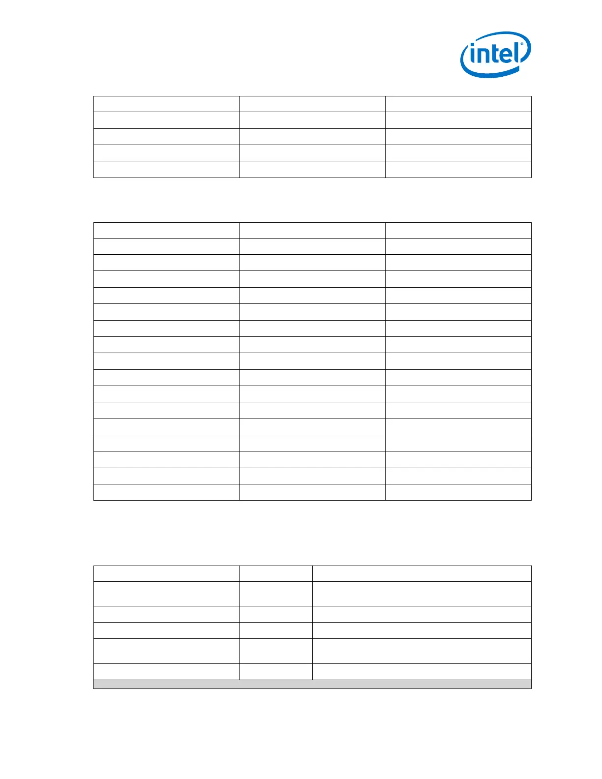
Table 138. RX XGMII Mapping to Standard SDR XGMII Interface
The 72-bit RX XGMII data bus format is different from the standard SDR XGMII interface. This table shows the
mapping of this non-standard format to the standard SDR XGMII interface.
Signal Name XGMII Signal Name Description
xgmii_rx_dc[7:0] xgmii_sdr_data[7:0]
Lane 0 data
xgmii_rx_dc[8] xgmii_sdr_ctrl[0]
Lane 0 control
xgmii_rx_dc[16:9] xgmii_sdr_data[15:8]
Lane 1 data
xgmii_rx_dc[17] xgmii_sdr_ctrl[1]
Lane 1 control
xgmii_rx_dc[25:18] xgmii_sdr_data[23:16]
Lane 2 data
xgmii_rx_dc[26] xgmii_sdr_ctrl[2]
Lane 2 control
xgmii_rx_dc[34:27] xgmii_sdr_data[31:24]
Lane 3 data
xgmii_rx_dc[35] xgmii_sdr_ctrl[3]
Lane 3 control
xgmii_rx_dc[43:36] xgmii_sdr_data[39:32]
Lane 4 data
xgmii_rx_dc[44] xgmii_sdr_ctrl[4]
Lane 4 control
xgmii_rx_dc[52:45] xgmii_sdr_data[47:40]
Lane 5 data
xgmii_rx_dc[53] xgmii_sdr_ctrl[5]
Lane 5 control
xgmii_rx_dc[61:54] xgmii_sdr_data[55:48]
Lane 6 data
xgmii_rx_dc[62] xgmii_sdr_ctrl[6]
Lane 6 control
xgmii_rx_dc[70:63] xgmii_sdr_data[63:56]
Lane 7 data
xgmii_rx_dc[71] xgmii_sdr_ctrl[7]
Lane 7 control
2.6.4.6.4. GMII Interface
The GMII interface signals drive data to and from the PHY.
Table 139. GMII Interface Ports
Signal Name Direction Description
gmii_tx_d[7:0]
Input Data to be encoded and sent to the link partner. This signal
is clocked with tx_clkout.
gmii_tx_en
Input
The GMII TX control signal. Synchronous to tx_clkout.
gmii_tx_err
Input
The GMII TX error signal. Synchronous to tx_clkout.
gmii_rx_d[7:0]
Output Data to be encoded and sent to the link partner. This signal
is clocked with tx_clkout.
gmii_rx_dv
Output
The GMII RX control signal. Synchronous to tx_clkout.
continued...
2. Implementing Protocols in Arria 10 Transceivers
UG-01143 | 2018.06.15
Intel
®
Arria
®
10 Transceiver PHY User Guide
177
 Loading...


