Note: Refer to the Gen1 and Gen2 Clock Compensation section for waveforms.
Related Information
Gen1 and Gen2 Clock Compensation on page 234
2.7.2.2.5. Gen3 Power State Management
The PCIe base specification defines low power states for PHY layer devices to minimize
power consumption. The Gen3 PCS does not implement these power saving measures,
except when placing the transmitter driver in electrical idle in the low power state. In
the P2 low power state, the transceivers do not disable the PIPE block clock.
Figure 99. P1 to P0 Transition
The figure below shows the transition from P1 to P0 with completion provided by pipe_phy_status.
P1 P0
tx_coreclkin
pipe_powerdown
pipe_phy_status
2.7.2.2.6. CDR Control
The CDR control block performs the following functions:
• Controls the PMA CDR to obtain bit and symbol alignment
• Controls the PMA CDR to deskew within the allocated time
• Generates status signals for other PCS blocks
The PCIe base specification requires that the receiver L0s power state exit time be a
maximum of 4 ms for Gen1, 2 ms for Gen2, and 4 ms for Gen3 signaling rates. The
transceivers have an improved CDR control block to accommodate fast lock times.
Fast lock times are necessary for the CDR to relock to the new multiplier/divider
settings when entering or exiting Gen3 speeds.
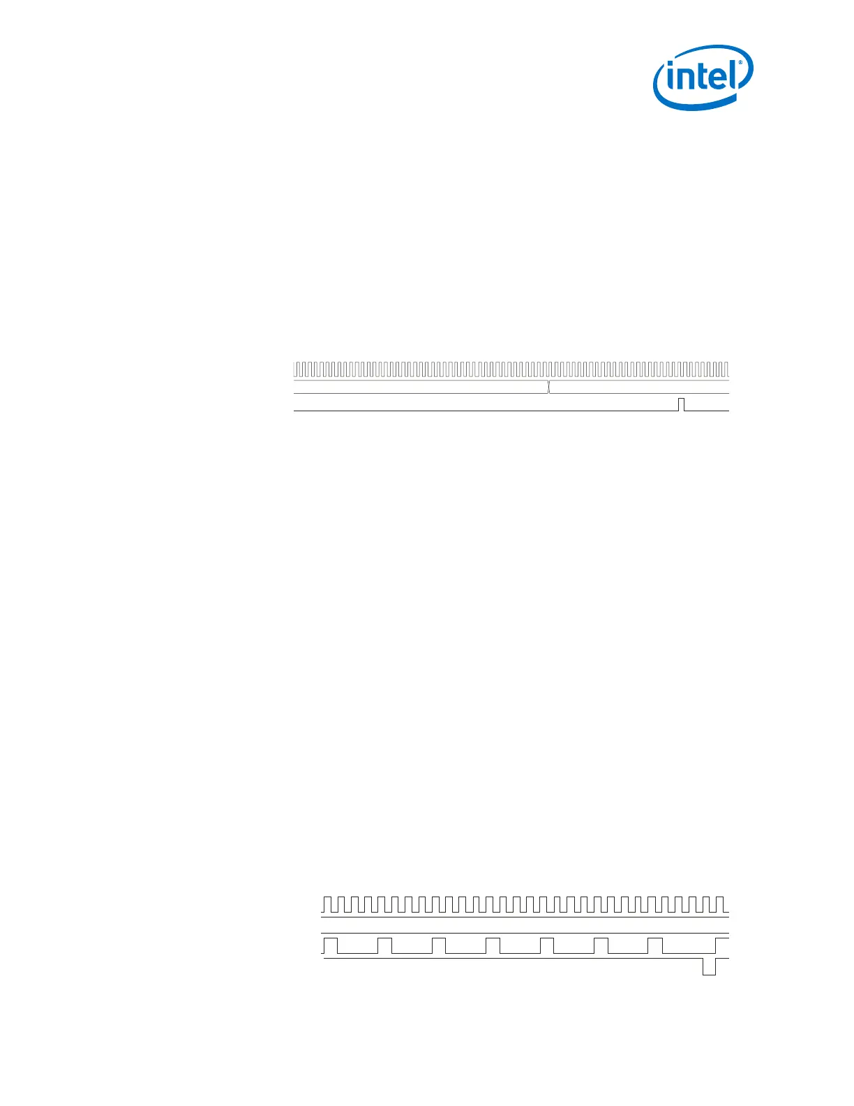
2.7.2.2.7. Gearbox
As per the PIPE 3.0 specification, for every 128 bits that are moved across the Gen3
PCS, the PHY must transmit 130 bits of data. Intel uses the pipe_tx_data_valid
signal every 16 blocks of data to transmit the built-up backlog of 32 bits of data.
The 130-bit block is received as follows in the 32-bit data path: 34 (32+2-bit sync
header), 32, 32, 32. During the first cycle, the gearbox converts the 34-bit input data
to 32-bit data. During the next three clock cycles, the gearbox merges bits from
adjacent cycles. For the gearbox to work correctly, a gap must be provided in the data
for every 16 shifts because each shift contains two extra bits for converting the initial
34 bits to 32 bits in the gearbox. After 16 shifts, the gearbox has an extra 32 bits of
data that are transmitted out. This requires a gap in the input data stream, which is
achieved by driving pipe_tx_data_valid low for one cycle after every 16 blocks of
data.
Figure 100. Gen3 Data Transmission
10
tx_coreclkin
pipe_tx_sync_hdr
pipe_tx_blk_start
pipe_tx_data_valid
2. Implementing Protocols in Arria 10 Transceivers
UG-01143 | 2018.06.15
Intel
®
Arria
®
10 Transceiver PHY User Guide
239