The rate match FIFO can insert as many pairs of skip patterns into a cluster
necessary to avoid the rate match FIFO from under running. The 10-bit skip
pattern can appear on the MSByte, the LSByte, or both, of the 20-bit word.
Figure 148. Rate Match FIFO Deletion with Four Skip Patterns Required for Deletion
/K28.5/ is the control pattern and neutral disparity /K28.0/ is the skip pattern.
Dx.y K28.0 Dx.y K28.5 K28.0 K28.0 Dx.y
Dx.y K28.5 K28.0 Dx.y Dx.y
tx_parallel_data[19:10]
rx_parallel_data[9:0]
First Skip Cluster Second Skip Cluster
Two Pairs of Skip
Patterns Deleted
Dx.y K28.5
K28.5
K28.0 K28.0 Dx.ytx_parallel_data[9:0]
Dx.y K28.0 Dx.y
Dx.y
Dx.yrx_parallel_data[19:0]
K28.0
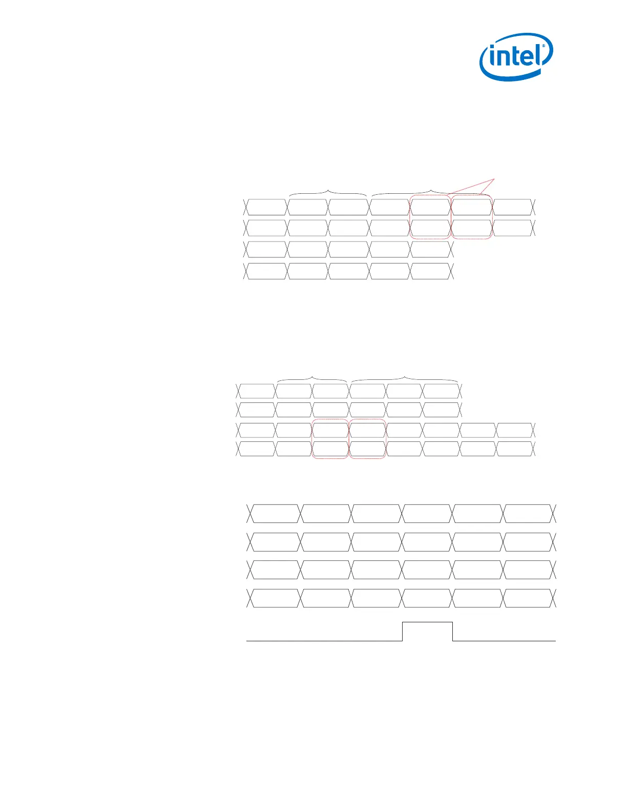
In the following figure, /K28.5/ is the control pattern and neutral disparity /K28.0/
is the skip pattern. The first skip cluster has a /K28.5/ control pattern in the
LSByte and /K28.0/ skip pattern in the MSByte of a clock cycle. The rate match
FIFO inserts pairs of skip patterns in this skip cluster to meet the three skip
pattern insertion requirement.
Figure 149. Rate Match FIFO Insertion with Four Skip Patterns Required for Insertion
Dx.y K28.0 Dx.y K28.5 K28.0 K28.0tx_parallel_data[19:10]
rx_parallel_data[9:0]
First Skip Cluster Second Skip Cluster
Dx.y K28.5 Dx.y Dx.y K28.0 K28.0tx_parallel_data[9:0]
rx_parallel_data[19:0]
Dx.y K28.0 K28.0 K28.0 Dx.y K28.5 K28.0
Dx.y K28.5 K28.0 K28.0 Dx.y Dx.y K28.0
K28.0
K28.0
The following figure shows the deletion of the 20-bit word D7D8.
Figure 150. Rate Match FIFO Becoming Full After Receiving the 20-Bit Word D5D6
D2 D4 D6 D10 D12 xx
D1 D3 D5 D9 D11
xx
rx_parallel_data[19:10]
rx_parallel_data[9:0]
rx_std_rmfifo_full
D2 D4 D6 D8 D10 D12
D1 D3 D5 D7 D9
D11
tx_parallel_data[19:0]
tx_parallel_data[9:0]
The following figure shows the insertion of two skip symbols.
2. Implementing Protocols in Arria 10 Transceivers
UG-01143 | 2018.06.15
Intel
®
Arria
®
10 Transceiver PHY User Guide
309