RL78/F13, F14 CHAPTER 2 PIN FUNCTIONS
R01UH0368EJ0210 Rev.2.10 84
Dec 10, 2015
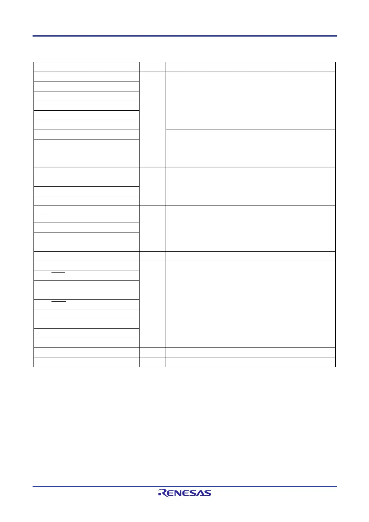
Table 2-6. Connection of Unused Pins (100-Pin Products of RL78/F14) (3/3)
Pin Name I/O Recommended Connection of Unused Pins
P100/ANI18 I/O Input: Independently connect to VDD or VSS via a resistor.
Output: Leave open.
P101/ANI19
P102/ANI20
P103/ANI21
P104/ANI22
P105/ANI23
P106/(LTXD1)
Input: Independently connect to EV
DD0 and EVDD1, or EVSS0 and EVSS1 via a
resistor.
Output: Leave open.
P107/(LRXD1)
P120/ANI25/TI07/TO07/TRDIOD0/SO01/
INTP4
P121/X1 Input Independently connect to VDD or VSS via a resistor.
P122/X2/EXCLK
P123/XT1
P124/XT2/EXCLKS
P125/ANI24/TI03/TO03/TRDIOB0/
SSI01/INTP1/SNZOUT1
I/O
Input: Independently connect to EV
DD0 and EVDD1, or EVSS0 and EVSS1 via a
resistor.
Output: Leave open.
P126/(TI01)/(TO01)
P127/(TI03)/(TO03)
P130/RESOUT Output Leave open.
P137/INTP0 Input Independently connect to VDD or VSS via a resistor.
P140/PCLBUZ0 I/O
Input: Independently connect to EV
DD0 and EVDD1, or EVSS0 and EVSS1 via a
resistor.
Output: Leave open.
P150/(SSI11)
P151/(SO11)
P152/(SI11)
P153/(SCK11)
P154/(SNZOUT7)
P155/(SNZOUT6)
P156/(SNZOUT5)
P157/(SNZOUT4)
RESET Input Connect to VDD directly or via a resistor.
REGC
Connect to VSS via a capacitor (0.47 to 1 µF).
Remark Functions in parentheses in the above table can be assigned via settings in the peripheral I/O redirection
registers (PIOR).

 Loading...


