RL78/F13, F14 CHAPTER 5 CLOCK GENERATOR
R01UH0368EJ0210 Rev.2.10 420
Dec 10, 2015
5.6.8 Time Required for Switchover of CPU Clock, Main System/PLL Select Clock, and Main System Clock
By setting bits 4 and 6 (MCM0, CSS) of the system clock control register (CKC), bits 0 to 2 (MDIV0 to MDIV2) of the f
MP
clock division register (MDIV), and bit 0 (SELLOSC) of the clock select register (CKSEL), the CPU clock can be switched
(between the main system/PLL select clock and the subsystem/low-speed on-chip oscillator select clock), the main
system/PLL select clock can be switched (between the main system clock and the PLL clock), the main system clock can
be switched (between the high-speed on-chip oscillator clock and the high-speed system clock), the subsystem/low-speed
on-chip oscillator select clock can be switched (between the subsystem clock and the low-speed on-chip oscillator clock),
and the frequency division ratio of the main system/PLL select clock can be changed.
The actual switchover operation is not performed immediately after rewriting to the CKC or MDIV register; operation
continues on the pre-switchover clock for several clocks. The subsystem/low-speed on-chip oscillator select clock is
switched immediately after rewriting to the CKSEL register.
Whether the CPU is operating on the main system/PLL select clock or the subsystem/low-speed on-chip oscillator select
clock can be ascertained using bit 7 (CLS) of the CKC register.
Whether the main system/PLL select clock is operating on the main system clock or the PLL clock can be ascertained
using bit 3 (SELPLLS) of the PLL status register (PLLSTS).
Whether the main system clock is operating on the high-speed on-chip oscillator clock or the high-speed system clock
can be ascertained using bit 5 (MCS) of the CKC register.
When the CPU clock is switched, the peripheral hardware clock is also switched.
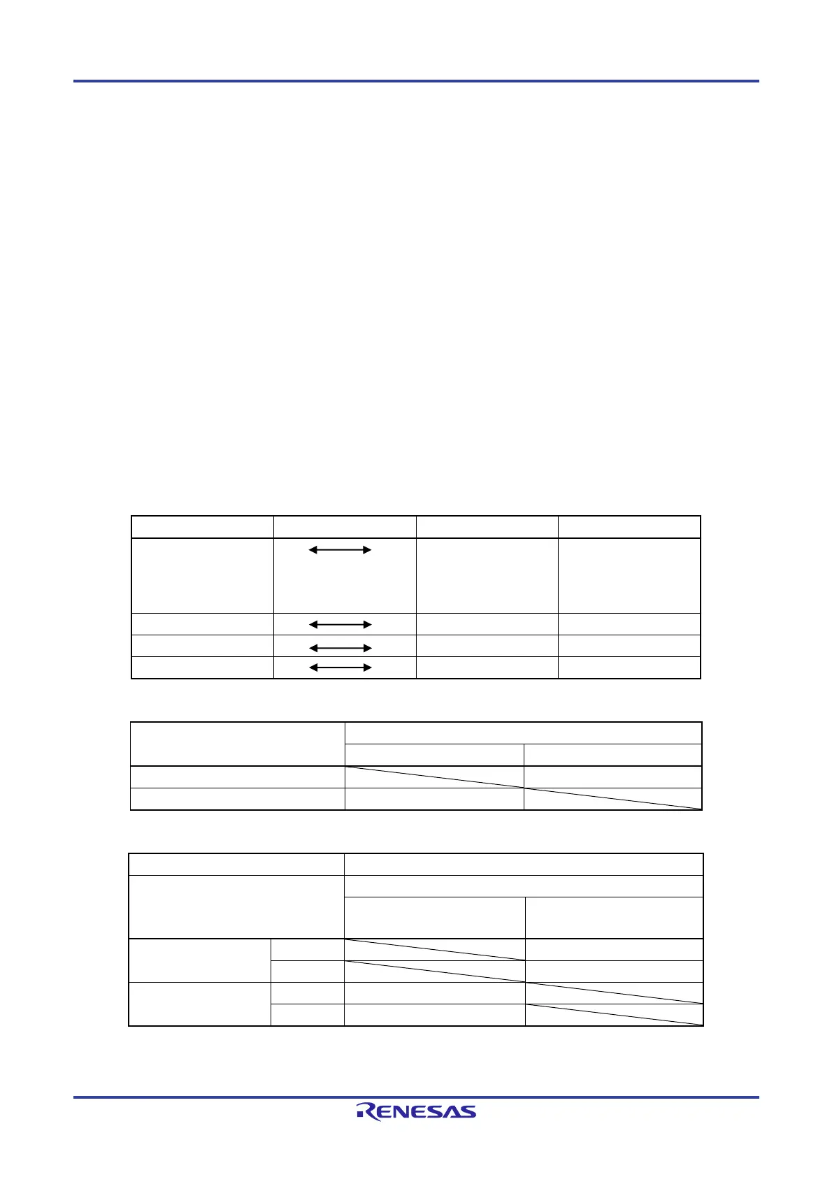
Table 5-4. Maximum Time Required for Clock Switchover
Clock A Switching directions Clock B Type
fMP
(change of the
frequency division
ratio)
f
MP Type 1 (Table 5-5)
fIH fMX Type 2 (Table 5-6)
fMP fSL Type 3 (Table 5-7)
fMAIN fPLL Type 4 (Table 5-8)
Table 5-5. Maximum Time Required for Type 1
Set Value Before Switchover Set Value After Switchover
Clock A Clock B
Clock A 1 + fA/fB clock
Clock B 1 + fB/fA clock
Table 5-6. Maximum Time Required for Type 2 (1)
Note1
Set Value Before Switchover Set Value After Switchover
MCM0 MCM0
0
(f
MAIN = fIH)
1
(fMAIN = fMX)
0
(f
MAIN = fIH)
f
MX fIH 3 clocks
fMX fIH 3 fIH/fMX clock
1
(f
MAIN = fMX)
f
MX fIH 3 fMX/fIH clock
fMX fIH 3 clocks
Note 1. For fIH ≤ 32 MHz
(Remarks are listed on the next page.)

 Loading...


