RL78/F13, F14 CHAPTER 26 VOLTAGE DETECTOR
R01UH0368EJ0210 Rev.2.10 1563
Dec 10, 2015
26.3.1 Voltage detection register (LVIM)
This register is used to specify whether to enable or disable rewriting the voltage detection level register (LVIS), as well
as to check the LVD output mask status.
This register can be set by a 1-bit or 8-bit memory manipulation instruction.
Reset signal generation clears this register to 00H
Note 1
.
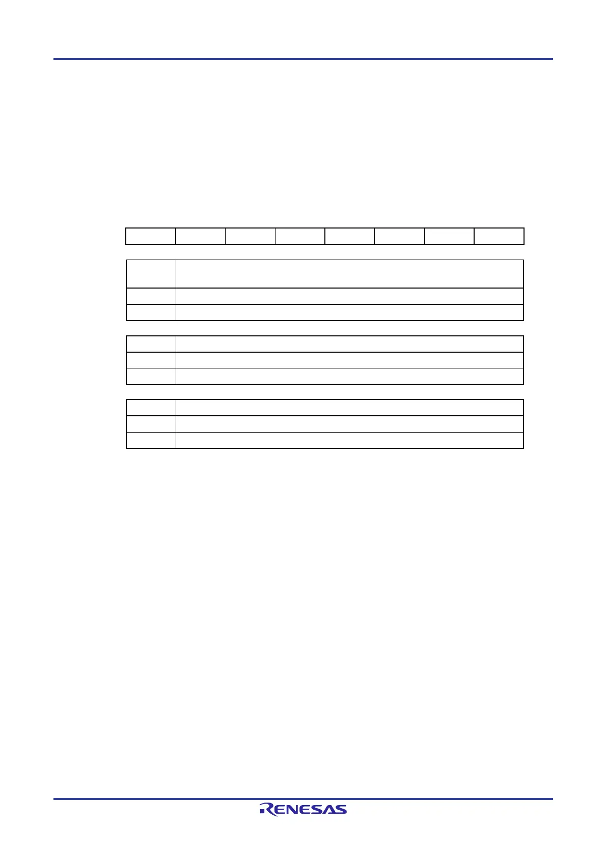
Figure 26-2. Format of Voltage Detection Register (LVIM)
Address: FFFA9H After reset: 00H
Note 1
R/W
Note 2
Symbol <7> 6 5 4 3 2 <1> <0>
LVIM LVISEN 0 0 0 0 0 LVIOMSK LVIF
LVISEN
Specification of whether to enable or disable rewriting the voltage detection level
register (LVIS)
0 Disabling rewriting
1
Enabling rewriting
Note 3
LVIOMSK Mask status flag of LVD output
0 Mask is invalid
1
Mask is valid
Note 4
LVIF Voltage detection flag
0 Supply voltage (VDD) detection voltage (VLVD), or when LVD operation is disabled
1 Supply voltage (VDD) < detection voltage (VLVD)
Notes 1. The reset value changes depending on the reset source.
If the LVIS register is reset by LVD, it is not reset but holds the current value.
LVISEN is cleared to 0 by any reset other than one due to LVD.
2. Bits 0 and 1 are read-only.
3. This can only be set when LVIMDS1 and LVIMDS0 are set to 1 and 0 (interrupt and reset mode) by the
option byte.
4. LVIOMSK bit is automatically set to 1 in the following periods and reset or interruption by LVD is masked.
Period during LVISEN = 1
Waiting period from the time when LVD interrupt is generated until LVD detection voltage becomes stable
Waiting period from the time when the value of LVILV bit changes until LVD detection voltage becomes
stable

 Loading...


