RL78/F13, F14 CHAPTER 6 TIMER ARRAY UNIT
R01UH0368EJ0210 Rev.2.10 454
Dec 10, 2015
6.3.8 Timer input select register 0 (TIS0)
The TIS0 register selects an input source of the timer array unit 0.
Set the TIS0 register by an 8-bit memory manipulation instruction.
Reset signal generation clears this register to 00H.
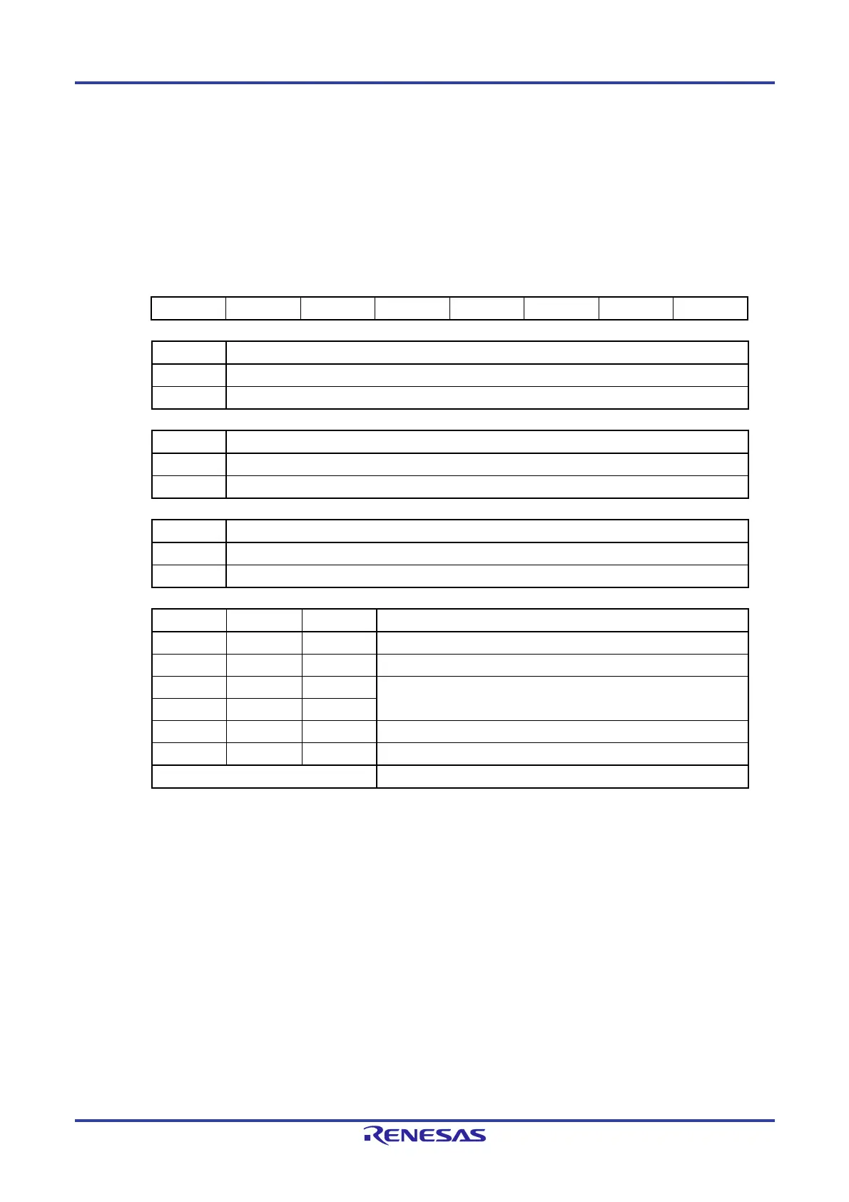
Figure 6-18. Format of Timer Input Select Register 0 (TIS0)
Address: F0074H After reset: 00H R/W
Symbol 7 6 5 4 3 2 1 0
TIS0 TIS07
Note 1
TIS06
Note 1
0 TIS04
Note 2
0 TIS02 TIS01 TIS00
TIS07
Note 1
Selection of timer input used with channel 3 of timer array unit 0
0 Input signal of timer input pin (TI03)
1 Event input signal from ELC
Note 3
TIS06
Note 1
Selection of timer input used with channel 2 of timer array unit 0
0 Input signal of timer input pin (TI02)
1 Event input signal from ELC
Note 3
TIS04
Note 2
Selection of timer input used with channel 0 of timer array unit 0
0 Input signal of timer input pin (TI00)
1 Event input signal from ELC
Note 3
TIS02 TIS01 TIS00 Selection of timer input used with channel 1 of timer array unit 0
0 0 0 Input signal of timer input pin (TI01)
0 0 1 Event input signal from ELC
Note 3
0 1 0 Input signal of timer input pin (TI01)
0 1 1
1 0 0 Low-speed on-chip oscillator clock (fIL)
1 0 1 Sub/low-speed on-chip oscillator select clock (fSL)
Other than above Setting prohibited
Notes 1. Provided only in products of group E. Write "0" when writing to the timer input select register 0 (TIS0) of the
other products.
2. Provided only in products of groups D and E. Write "0" when writing to the timer input select register 0 (TIS0)
of the other products.
3. Provided only in products of groups D and E. Do not set in the other products.
Cautions 1. When selecting an event input signal from the ELC using timer input select register 0 (TIS0), select
f
CLK using timer clock select register 0 (TPS0).
2. Do not change the select bit of the timer input while inputting data to the TImn pin (m = 0, 1; n = 0
to 7).
3. Each of the high-level and low-level widths of the timer input to be selected should be (1/f
MCK + 10
ns) or more. So, the TIS02 bit cannot be set to 1 when f
SL is selected as fCLK (the CSS bit in the CKC
register is set to 1).

 Loading...


