RL78/F13, F14 CHAPTER 8 TIMER RD
R01UH0368EJ0210 Rev.2.10 573
Dec 10, 2015
8.2.4 Timer RD Start Register (TRDSTR)
Set the TRDSTR register by an 8-bit memory manipulation instruction. See 8. 5. 1 (1) TRDSTR Register in 8.5 Notes
on Timer RD.
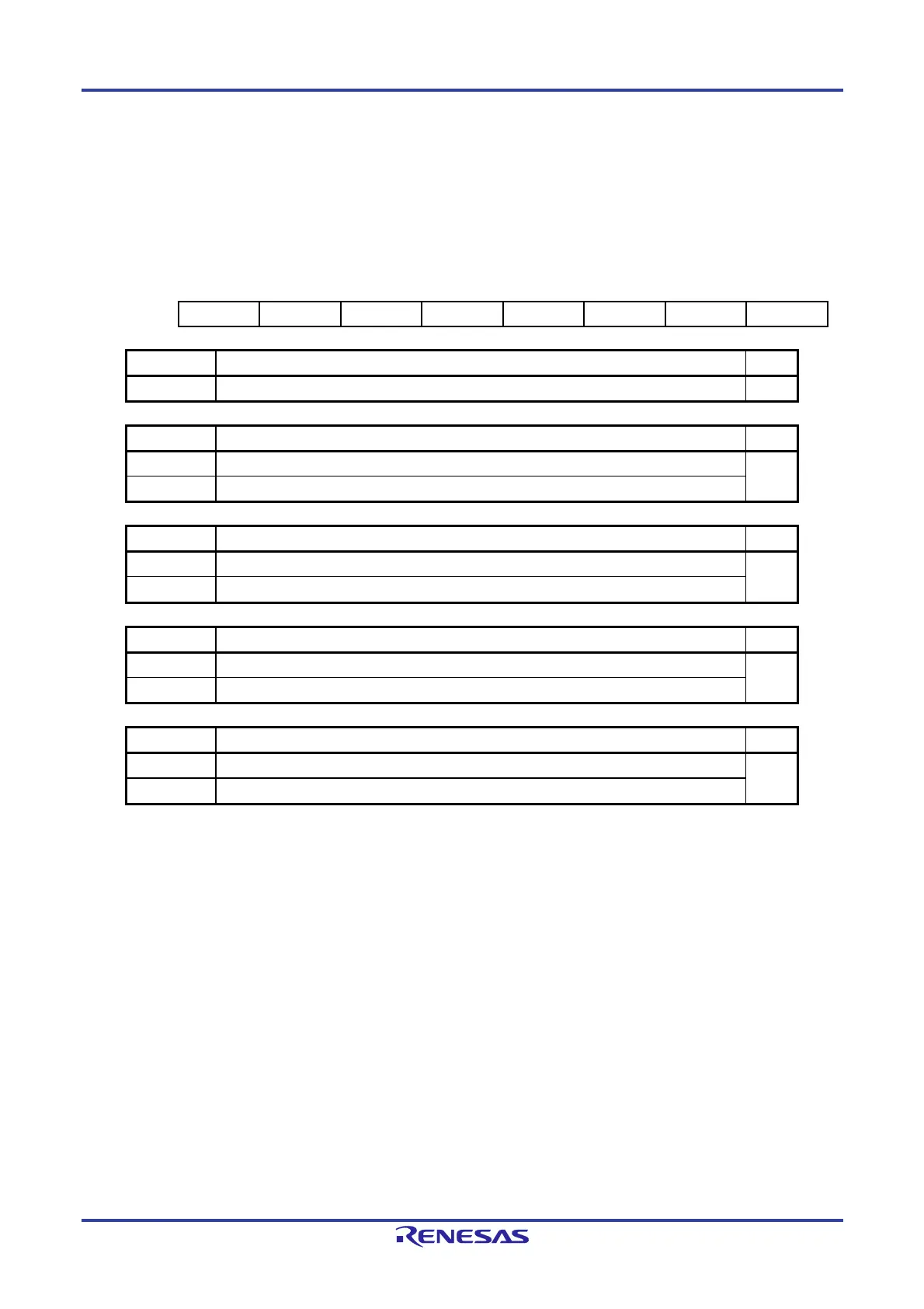
Figure 8-5. Format of Timer RD Start Register (TRDSTR)
Address: F0263H After Reset: 0CH
Note 1
Symbol 7 6 5 4 3 2 1 0
TRDSTR — — — — CSEL1 CSEL0 TSTART1 TSTART0
Bits 7 to 4 Nothing is assigned R/W
—
The write value must be 0. The read value is 0.
R
CSEL1
TRD1 count operation select
Note 2
R/W
0
Count stops at compare match with TRDGRA1 register
R/W
1
Count continues after compare match with TRDGRA1 register
Note 3
CSEL0 TRD0 count operation select R/W
0
Count stops at compare match with TRDGRA0 register
R/W
1
Count continues after compare match with TRDGRA0 register
Note 3
TSTART1
TRD1 count start flag
Notes 4, 5
R/W
0
Count stops
R/W
1
Count starts
TSTART0
TRD0 count start flag
Notes 6, 7
R/W
0
Count stops
R/W
1
Count starts
Notes 1. The value after reset is undefined when FRQSEL4 = 1 in the user option byte (000C2H/020C2H) and
TRD0EN = 0 in the PER1 register. If it is necessary to read the initial value, set f
CLK to fIH and TRD0EN =
1 before reading.
2. Do not use in PWM3 mode.
3. Set to 1 for the input capture function.
4. Write 0 to the TSTART1 bit while the CSEL1 bit is set to 1.
5. When the CSEL1 bit is 0 and a compare match signal (TRDIOA1) is generated, this flag is set to 0 (count
stops).
6. Write 0 to the TSTART0 bit while the CSEL0 bit is set to 1.
7. When the CSEL0 bit is 0 and a compare match signal (TRDIOA0) is generated, this flag is set to 0 (count
stops).

 Loading...


