RL78/F13, F14 CHAPTER 12 A/D CONVERTER
R01UH0368EJ0210 Rev.2.10 735
Dec 10, 2015
12.5 Input Voltage and Conversion Results
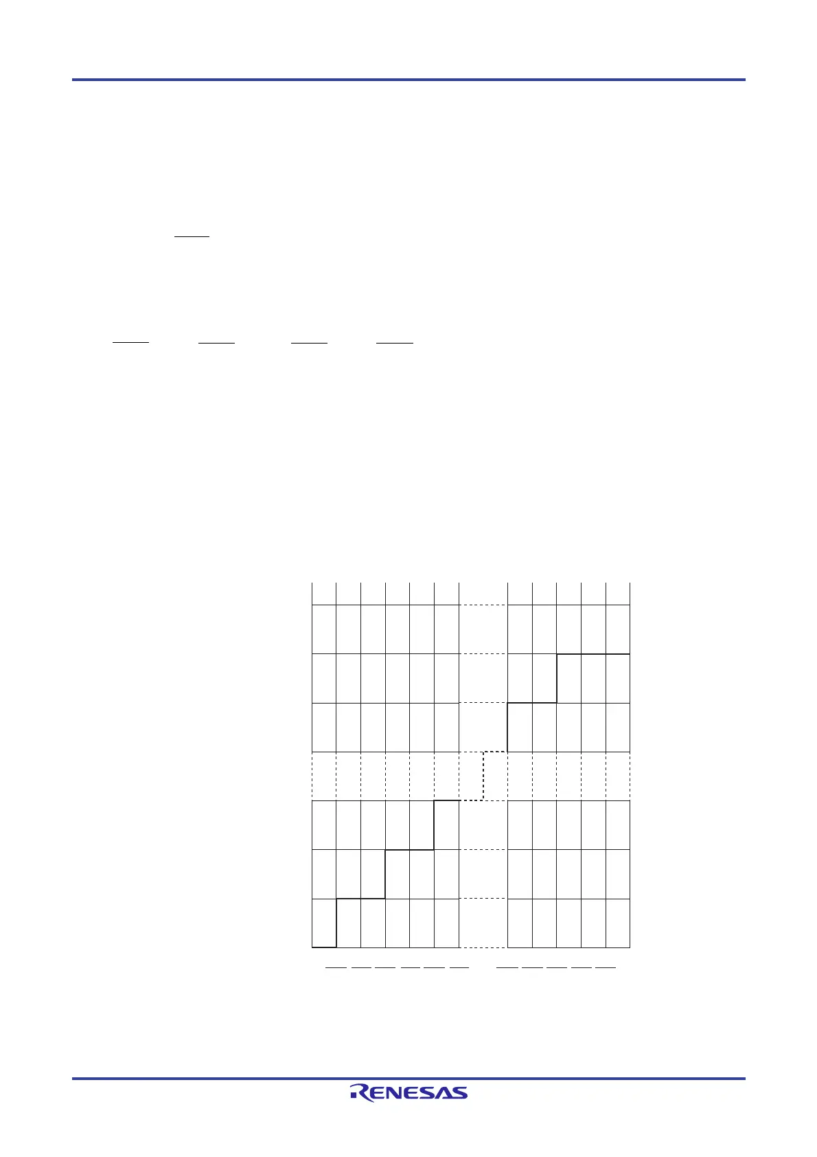
The relationship between the analog input voltage input to the analog input pins (ANI0 to ANI23, ANI24 to ANI30) and
the theoretical A/D conversion result (stored in the 10-bit A/D conversion result register (ADCR)) is shown by the following
expression.
SAR = INT ( 1024 + 0.5)
ADCR = SAR 64
or
( 0.5) V
AIN < ( + 0.5)
where, INT( ): Function which returns integer part of value in parentheses
V
AIN: Analog input voltage
AV
REF: AVREF pin voltage
ADCR: A/D conversion result register (ADCR) value
SAR: Successive approximation register
Figure 12-21 shows the relationship between the analog input voltage and the A/D conversion result.
Figure 12-21 Relationship Between Analog Input Voltage and A/D Conversion Result
Remark AV
REF: The + side reference voltage of the A/D converter. This can be selected from AVREFP, the internal
reference voltage (1.45 V), and VDD.
1023
1022
1021
3
2
1
0
FFC0H
FF80H
FF40H
00C0H
0080H
0040H
0000H
A/D conversion result
SAR ADCR
1
2048
1
1024
3
2048
2
1024
5
2048
Input voltage/AV
REF
3
1024
2043
2048
1022
1024
2045
2048
1023
1024
2047
2048
1
VAIN
AV
REF
AVREF
1024
AVREF
1024
ADCR
64
ADCR
64

 Loading...


