RL78/F13, F14 CHAPTER 4 PORT FUNCTIONS
R01UH0368EJ0210 Rev.2.10 226
Dec 10, 2015
4.2.4 Port 4
Port 4 is an I/O port with an output latch. Port 4 can be set to the input mode or output mode in 1-bit units using port
mode register 4 (PM4). When the P40 to P47 pins are used as an input port, use of an on-chip pull-up resistor can be
specified in 1-bit units by pull-up resistor option register 4 (PU4).
For the P43 pin input, the threshold of the input buffer can be specified in 1-bit units using the port input threshold
control register 4 (PITHL4).
This port can also be used for external interrupt request input, timer I/O, comparator output, SNOOZE status output,
LIN serial data I/O, and data I/O for a flash memory programmer/debugger.
Reset signal generation sets this port to input mode.
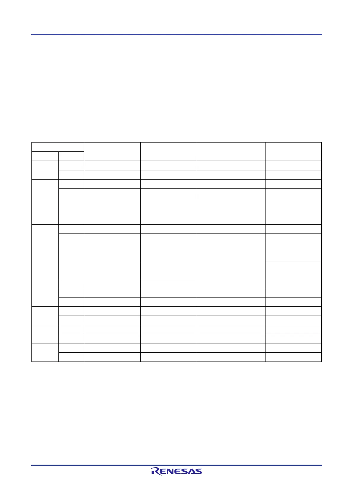
Table 4-8. Settings of Registers When Using Port 4
Pin name PM4x PITHL4x Alternate Function Setting
Note 6
Remark
Name I/O
P40 Input 1 – ×
Output 0 – ×
P41 Input 1 – ×
Output 0 – TRJIO0 output = 0
Note 1
TO10 output = 0
Note 2
VCOUT0 output = 0
Note 3
SNZOUT2 output = 0
Note 4
P42 Input 1 – ×
Output 0 – (LTXD0 = 1)
Note 5
P43 Input 1 0 × CMOS input
(Schmitt1 input)
1 × CMOS input
(Schmitt3 input)
Output 0 × ×
P44 Input 1 – ×
Output 0 – (TO07 output = 0)
Note 2
P45 Input 1 – ×
Output 0 – (TO10 output = 0)
Note 2
P46 Input 1 – ×
Output 0 – (TO12 output = 0)
Note 2
P47 Input 1 – ×
Output 0 – ×
Notes 1. When a pin sharing a timer input/output function of the timer RJ is to be used as a general-purpose port pin,
the TMOD2 to TMOD0 bits of the timer RJ mode register 0 (TRJMR0) must have the same setting as their
initial value or have a setting other than 001B.
2. When a pin sharing a timer output function of the timer array unit is to be used as a general-purpose port
pin, the TOmn bit of the timer output register m (TOm) and the TOEmn bit of the timer output enable
register m (TOEm) corresponding to the target unit and channel must have the same setting as in the initial
state (m = 0, 1, n = 0 to 7).
3. When a pin sharing the comparator output function is to be used as a general-purpose port pin, the COE bit
of the comparator control register (CMPCTL) must have the same setting as its initial value.
4. When a pin sharing the SNOOZE status output function is to be used as a general-purpose port pin, the
OUTEN0 to OUTEN7 bits of the SNOOZE status output control registers 0, 1, 2, 3 (PSNZCNT0, 1, 2, 3)
must have the same setting as its initial value.
 Loading...


