RL78/F13, F14 CHAPTER 12 A/D CONVERTER
R01UH0368EJ0210 Rev.2.10 706
Dec 10, 2015
12.3.1 Peripheral enable register 0 (PER0)
This register is used to enable or disable supplying the clock to the peripheral hardware. Clock supply to a hardware
macro that is not used is stopped in order to reduce the power consumption and noise.
When the A/D converter is used, be sure to set bit 5 (ADCEN) of this register to 1.
The PER0 register can be set by a 1-bit or 8-bit memory manipulation instruction.
Reset signal generation clears this register to 00H.
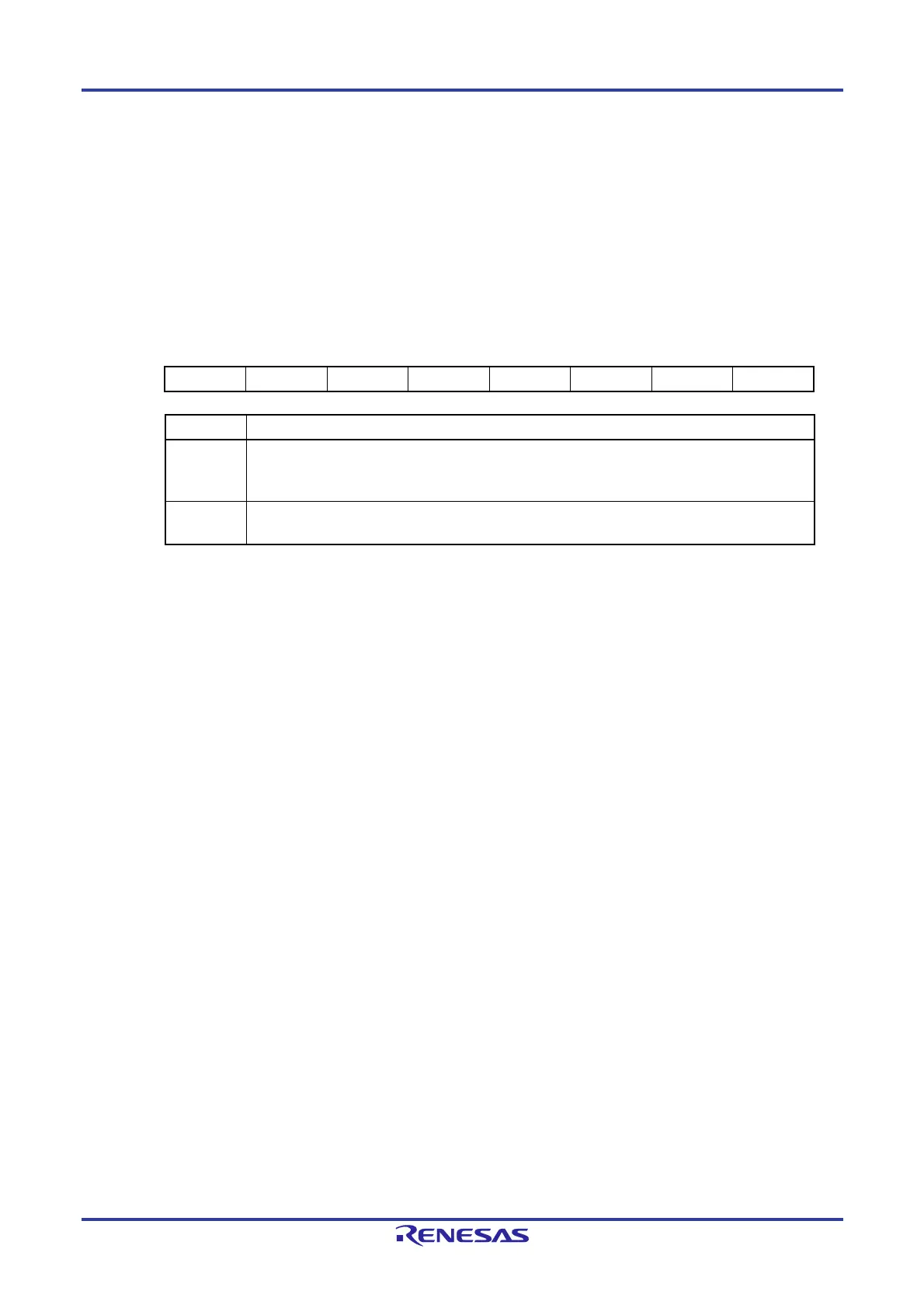
Figure 12-2. Format of Peripheral Enable Register 0 (PER0)
Address: F00F0H After reset: 00H R/W
Symbol <7> 6 <5> <4> <3> <2> <1> <0>
PER0 RTCEN 0 ADCEN IICA0EN SAU1EN SAU0EN TAU1EN TAU0EN
ADCEN Control of A/D converter input clock supply
0
Stops input clock supply.
SFR used by the A/D converter cannot be written.
The A/D converter is in the reset status.
1
Enables input clock supply.
SFR used by the A/D converter can be read/written.
Cautions 1. When setting the A/D converter, be sure to set the ADCEN bit to 1 first. If ADCEN = 0,
writing to a control register of the A/D converter is ignored, and, even if the register is read,
only the default value is read (except for port mode registers 3, 7 to 10, 12 (PM3, PM7 to
PM10, PM12), port mode control registers 7, 9, and 12 (PMC7, PMC9, PMC12), and A/D port
configuration register (ADPC)).
2. Be sure to clear the following bits to 0.
Bits 1, 3, 4, and 6 in the RL78/F13 (LIN incorporated) products with 20, 30, 32, 48, or 64
pins and 16 Kbytes to 64 Kbytes of code flash memory
Bits 4 and 6 in 30-pin products of the RL78/F13 (CAN and LIN incorporated) and in 30-pin
products of the RL78/F14
Bit 6 in the products other than above

 Loading...


