RL78/F13, F14 CHAPTER 6 TIMER ARRAY UNIT
R01UH0368EJ0210 Rev.2.10 455
Dec 10, 2015
6.3.9 Timer input select register 1 (TIS1)
The TIS1 register selects an input source of the timer array unit 0.
The TIS17 and TIS16 bits in the TIS1 register are used in conjunction with the serial array unit to implement the LIN-bus
communication operation in channel 7. When the TIS17 and TIS16 bits are set to 1 and 0 respectively, the input signal on
the serial data input pin (RxD0) is selected as the timer input.
Set the TIS17 and TIS16 bits at the same time as setting the ISC0 bit in the ISC register (input switch control register).
Set the TIS1 register by an 8-bit memory manipulation instruction.
Reset signal generation clears this register to 00H.
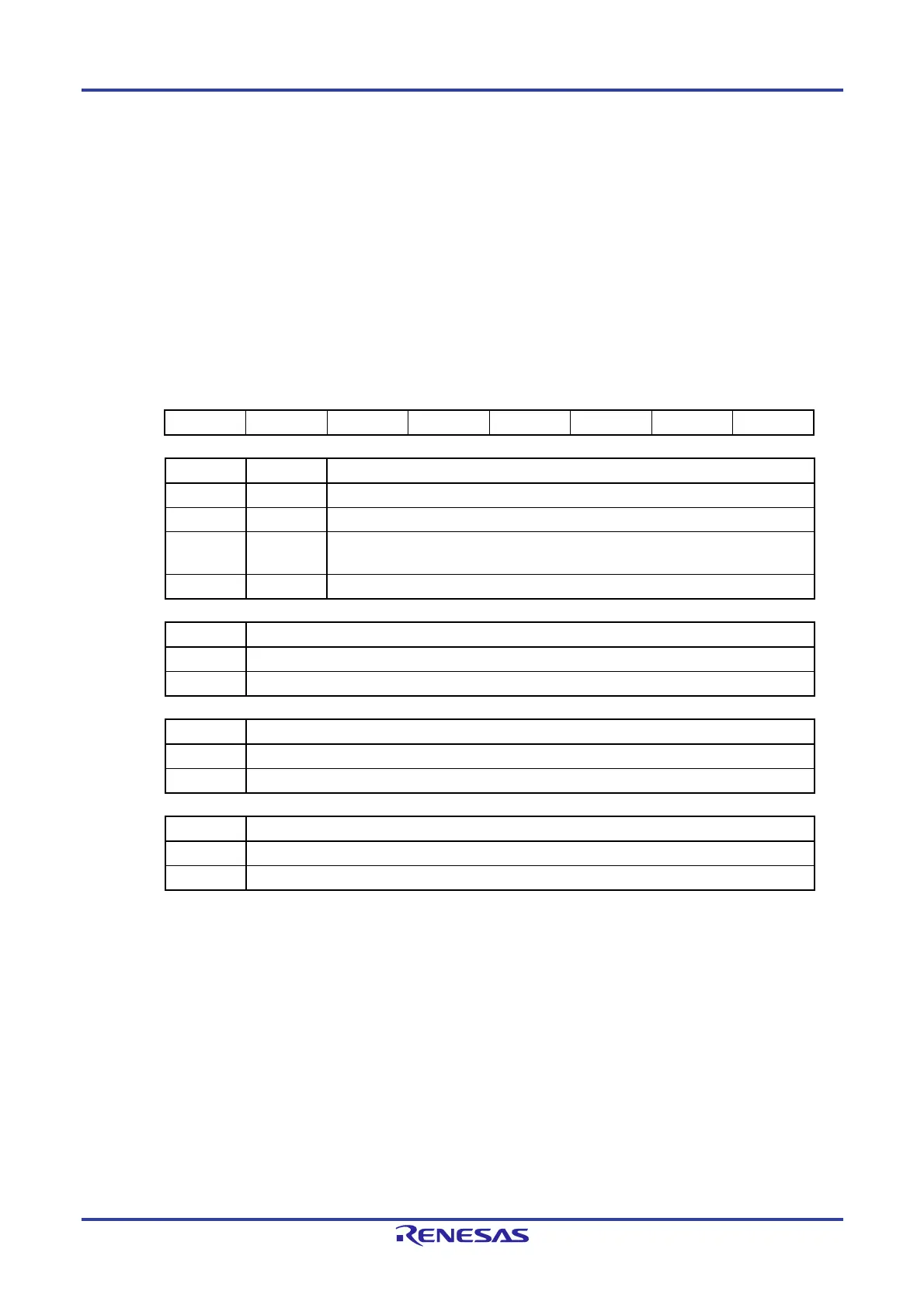
Figure 6-19. Format of Timer Input Select Register 1 (TIS1)
Address: F0075H After reset: 00H R/W
Symbol 7 6 5 4 3 2 1 0
TIS1 TIS17 TIS16 0 TIS14 0 TIS12 0 TIS10
TIS17 TIS16 Selection of timer input used with channel 7 of timer array unit 0
0 0 Input signal of timer input pin (TI07)
0 1 RTC1HZ output signal
1 0
RxD0 pin (detection of the wake-up signal and measurement of the low-level width of
the sync break field and the pulse width of the sync field)
1 1 Setting prohibited
TIS14 Selection of timer input used with channel 6 of timer array unit 0
0 Input signal of timer input pin (TI06)
1 RTC1HZ output signal
TIS12 Selection of timer input used with channel 5 of timer array unit 0
0 Input signal of timer input pin (TI05)
1 Input signal of timer input pin (TI03)
TIS10 Selection of timer input used with channel 4 of timer array unit 0
0 Input signal of timer input pin (TI04)
1 Input signal of timer input pin (TI03)
Cautions 1. Do not change the select bit of the timer input while inputting data to the TImn pin (m = 0, 1; n = 0
to 7).
2. When selecting the RTC1HZ output signal for the clock source of the timer input used in channels
7 and 6 in the TAU, set the TIS17, TIS16, and TIS14 bits to 0, 1, and 1, respectively, and select the
RTC1HZ output signal for the timer input of channels 7 and 6.
Remark Set the TIS17 and TIS16 bits to 1 and 0 respectively and select the input signal of the RxD0 pin before using
the LIN-bus communication.

 Loading...


