RL78/F13, F14 CHAPTER 19 DTC
R01UH0368EJ0210 Rev.2.10 1431
Dec 10, 2015
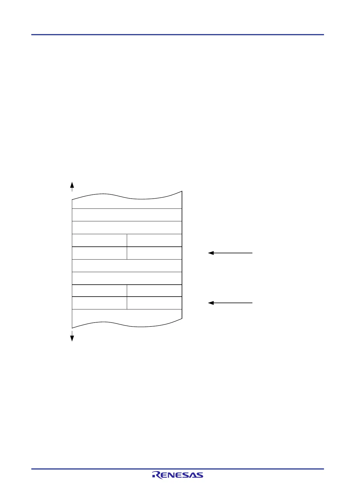
19.2.2 DTC Control Data Allocation
Control data is allocated beginning with each start address in the order: Registers DTCCRj, DTBLSj, DTCCTj, DTRLDj,
DTSARj, and DTDARj (j = 0 to 23).
The higher 8 bits for start addresses 0 to 23 are set by the DTCBAR register, and the lower 8 bits are separately set
according to the vector table assigned to each activation source.
Figure 19-3 shows an example of DTC control data allocation when the DTCBAR register is set to FBH.
Cautions
Change the data in registers DTCCRj, DTBLSj, DTCCTj, DTRLDj, DTSARj, and DTDARj when the
corresponding bit among bits DTCENi0 to DTCENi7 (i = 0 to 5
Note
) in the DTCENi register is set to 0 (DTC
activation disabled).
Do not access DTCCRj, DTBLSj, DTCCTj, DTRLDj, DTSARj, or DTDARj using a DTC transfer.
Note Products of groups A, B, C, and D: i = 0 to 4
Products of group E: i = 0 to 5
Figure 19-3. DTC Control Data Allocation
FFFFFH
DTDAR1 register
DTSAR1 register
DTRLD1 register DTCCT1 register
DTBLS1 register DTCCR1 register
DTDAR0 register
DTSAR0 register
DTRLD0 register DTCCT0 register
DTBLS0 register
DTCCR0 register
F0000H
Start address of DTC
control data 0
Start address of DTC
control data 1
Lower addressHigher address
FFB48H
FFB40H

 Loading...


