RL78/F13, F14 CHAPTER 18 CAN INTERFACE (RS-CAN LITE)
R01UH0368EJ0210 Rev.2.10 1262
Dec 10, 2015
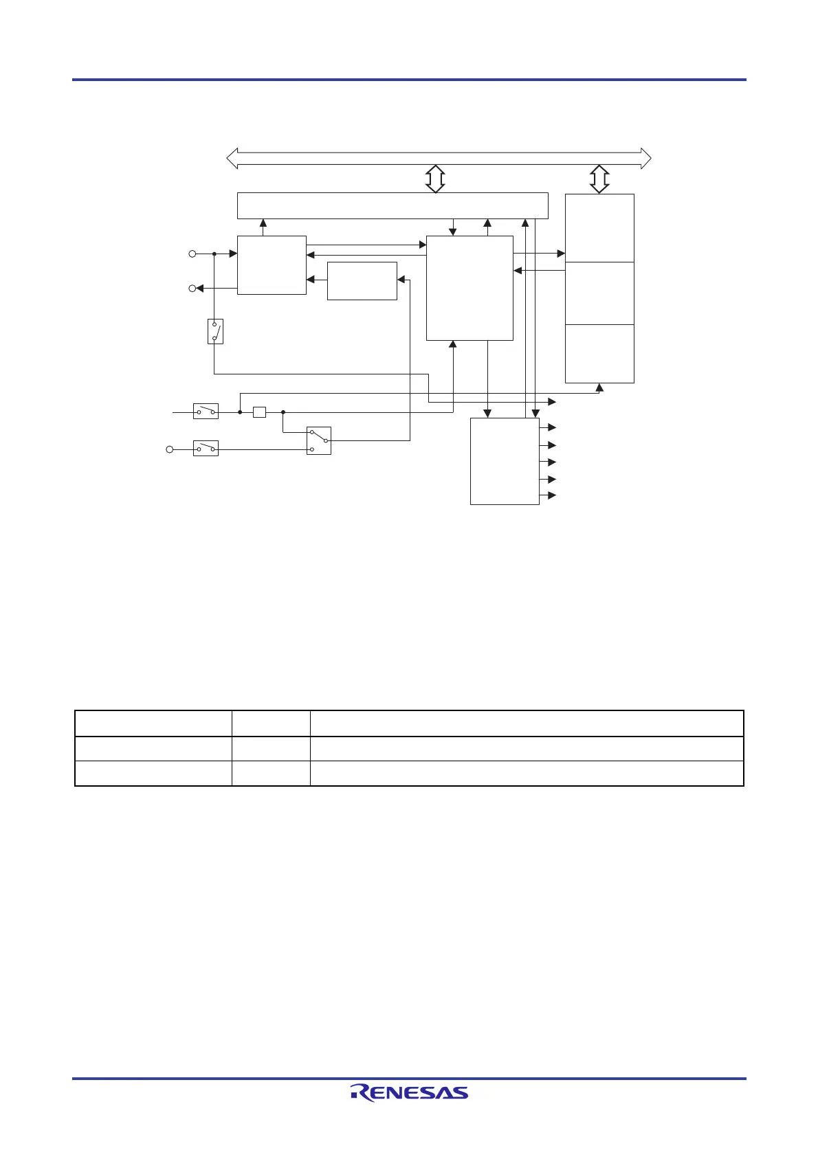
Figure 18-1. CAN Module Block Diagram (i = 0)
18.2 Input/Output Pins
Table 18-2 lists the I/O pins of the CAN module.
Table 18-2. I/O Pins of the CAN Module
Pin Name I/O Description
CRXDi Input Receive data input pins of the CAN communication function
CTXDi Output Transmit data output pins of the CAN communication function
CRXDi
CTXDi
DCS
CAN0EN
CAN0EN
CAN0MCKE
1/2
i = 0
BRP[9:0]: Bits in the CiCFGL register
DCS: Bit in the GCFGL register
f
CANTQi
: CANi Tq clock
f
CAN
: CAN clock
CAN0EN: Bit in the PER2 register
CAN0MCKE: Bit in the CANCKSEL register
CPU/peripheral
hardware clock
(f
CLK
)
X1 clock
(fx)
f
CAN
CAN global receive FIFO interrupt
CANi channel transmit interrupt
CANi transmit/receive FIFO receive interrupt
CANi channel error interrupt
CANi wakeup interrupt
Buffer RAM
FIFO RAM
Receive rule
table RAM
Acceptance filter
ID priority
transmission
controller
Timer
Baud rate prescaler
(BRP[9:0])
f
CANTQi
CAN-related registers
Peripheral bus
Protocol
controller
Interrupt
generator circuit
CAN global error interrupt
Remark

 Loading...


