RL78/F13, F14 CHAPTER 6 TIMER ARRAY UNIT
R01UH0368EJ0210 Rev.2.10 456
Dec 10, 2015
6.3.10 Timer input select register 2 (TIS2)
The TIS2 register selects an input source of the timer array unit 1.
Set the TIS2 register by an 8-bit memory manipulation instruction.
Reset signal generation clears this register to 00H.
This function is valid only for the Group E products.
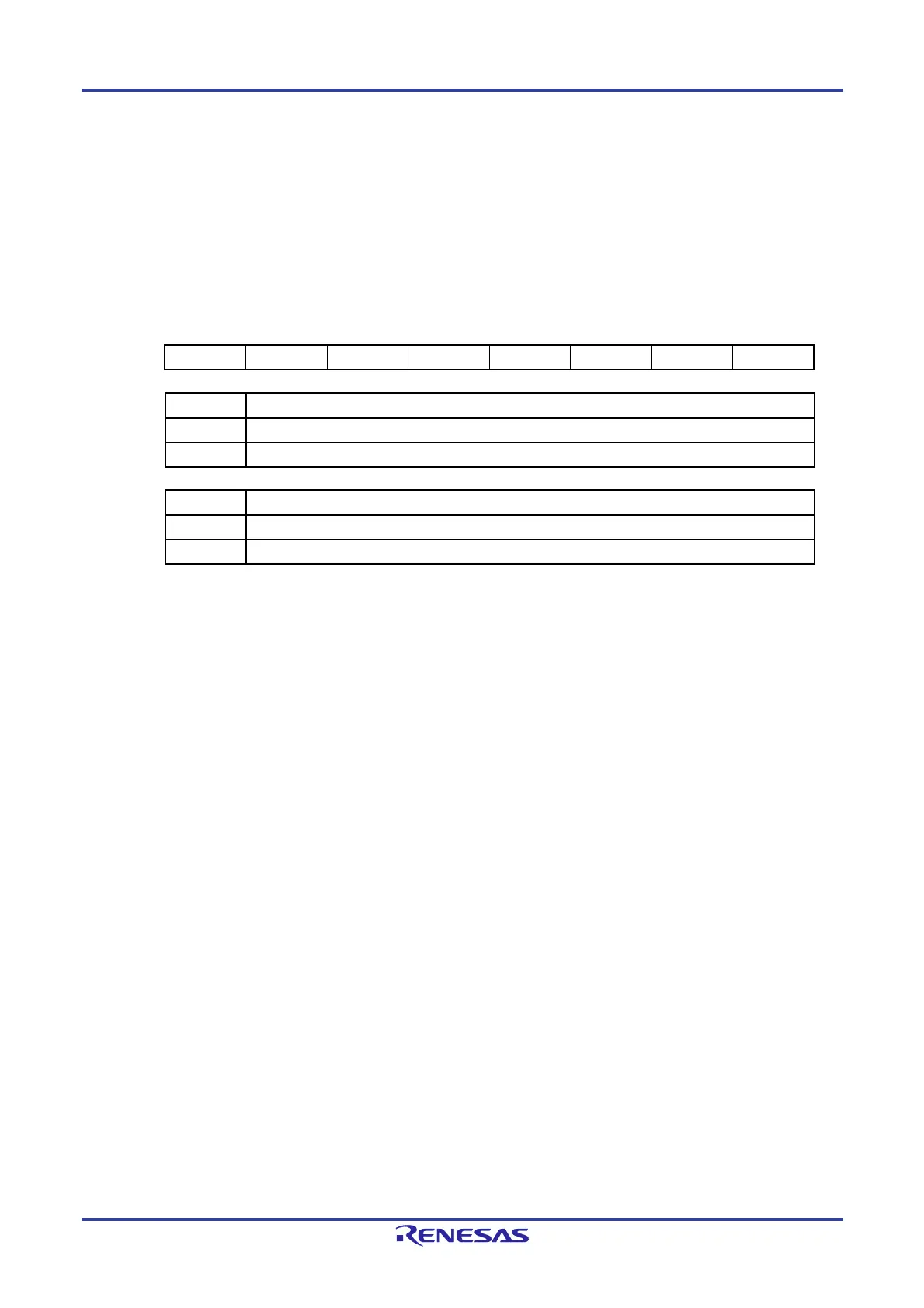
Figure 6-20. Format of Timer Input Select Register 2 (TIS2)
Address: F007AH After reset: 00H R/W
Symbol 7 6 5 4 3 2 1 0
TIS2 0 0 0 0 TIS23 TIS22 0 0
TIS22 Selection of timer input used with channel 6 of timer array unit 1
0 Input signal of timer input pin (TI16)
1 RTC1HZ output signal
TIS23 Selection of timer input used with channel 7 of timer array unit 1
0 Input signal of timer input pin (TI17)
1 RTC1HZ output signal
Cautions 1. Do not change the select bit of the timer input while inputting data to the TImn pin (m = 0, 1; n = 0
to 7).
2. When selecting the RTC1HZ output signal for the clock source of the timer input used in channels
7 and 6 in the TAU, set the TIS23 and TIS22 bits to 1 and select the RTC1HZ output signal for the
timer input of channels 7 and 6.

 Loading...


