RL78/F13, F14 CHAPTER 17 LIN/UART MODULE (RLIN3)
R01UH0368EJ0210 Rev.2.10 1212
Dec 10, 2015
(2) Reception of LIN Frames
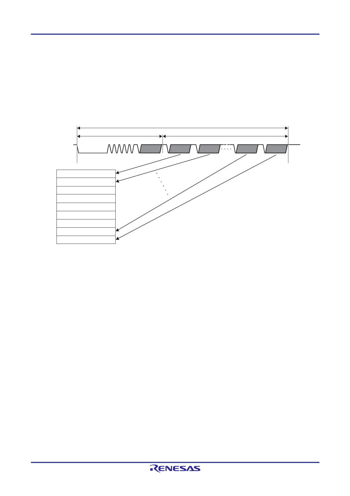
For an 8-byte reception, the contents of data areas 1 to 8 of the LIN frame is stored in registers LDBn1 to LDBn8, respectively,
upon receipt of a stop bit. In the case of a 4-byte reception, the contents of data areas 1 to 4 of the LIN frame are stored in
registers LDBn1 to LDBn4, respectively; however, no data is stored in registers LDBn5 to LDBn8. Also, the received
checksum data is stored in the LCBRn register.
Figure 17-17 depicts the LIN reception processing and the required buffer.
Figure 17-17. LIN Reception Processing and Required Buffer
(a) Reception of Data 1
When the reception of the first byte of data is finished, the D1RC flag in the LSTn register turns 1 (successful
data 1 reception).
Header
Frame
Response
Data 1
Data 2
Data 8
Checksum
Buffer
LDBn1 register
LDBn2 register
LDBn3 register
LDBn4 register
LDBn5 register
LDBn6 register
LDBn7 register
LDBn8 register
LCBRn register

 Loading...


