RL78/F13, F14 CHAPTER 30 FLASH MEMORY
R01UH0368EJ0210 Rev.2.10 1628
Dec 10, 2015
The dedicated flash memory programmer generates the following signals for the RL78/F13 and RL78/F14. See the
manual of PG-FP5, FL-PR5, or E1 on-chip debugging emulator for details.
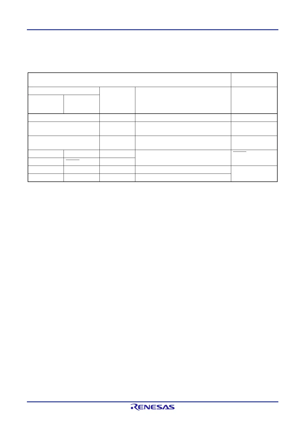
Table 30-2. Pin Connection
Dedicated Flash Memory Programmer
RL78/F13 and
RL78/F14
Signal Name I/O Pin Function Pin Name
PG-FP5,
FL-PR5
E1 on-chip
debugging
emulator
VDD I/O VDD voltage generation/power monitoring VDD
GND
Ground
V
SS, EVSS0
Note 1
, EVSS0
Note 2
, REGC
Note 3
EMVDD
Driving power for TOOL0 pin
V
DD, EVDD0
Note 1
,
EV
DD1
Note 2
/RESET
Output Reset signal RESET
RESET Output
TOOL0 I/O Transmit/receive signal TOOL0
SI/RxD
I/O Transmit/receive signal
Notes 1. 64, 80, 100-pin products only.
2. 100-pin products only.
3. Connect REGC pin to ground via a capacitor (0.47 to 1
F).
Caution The connection destination pins differ depending on the product. For details, see Table 30-1.

 Loading...


