RL78/F13, F14 CHAPTER 34 ELECTRICAL SPECIFICATIONS (GRADE L)
R01UH0368EJ0210 Rev.2.10 1711
Dec 10, 2015
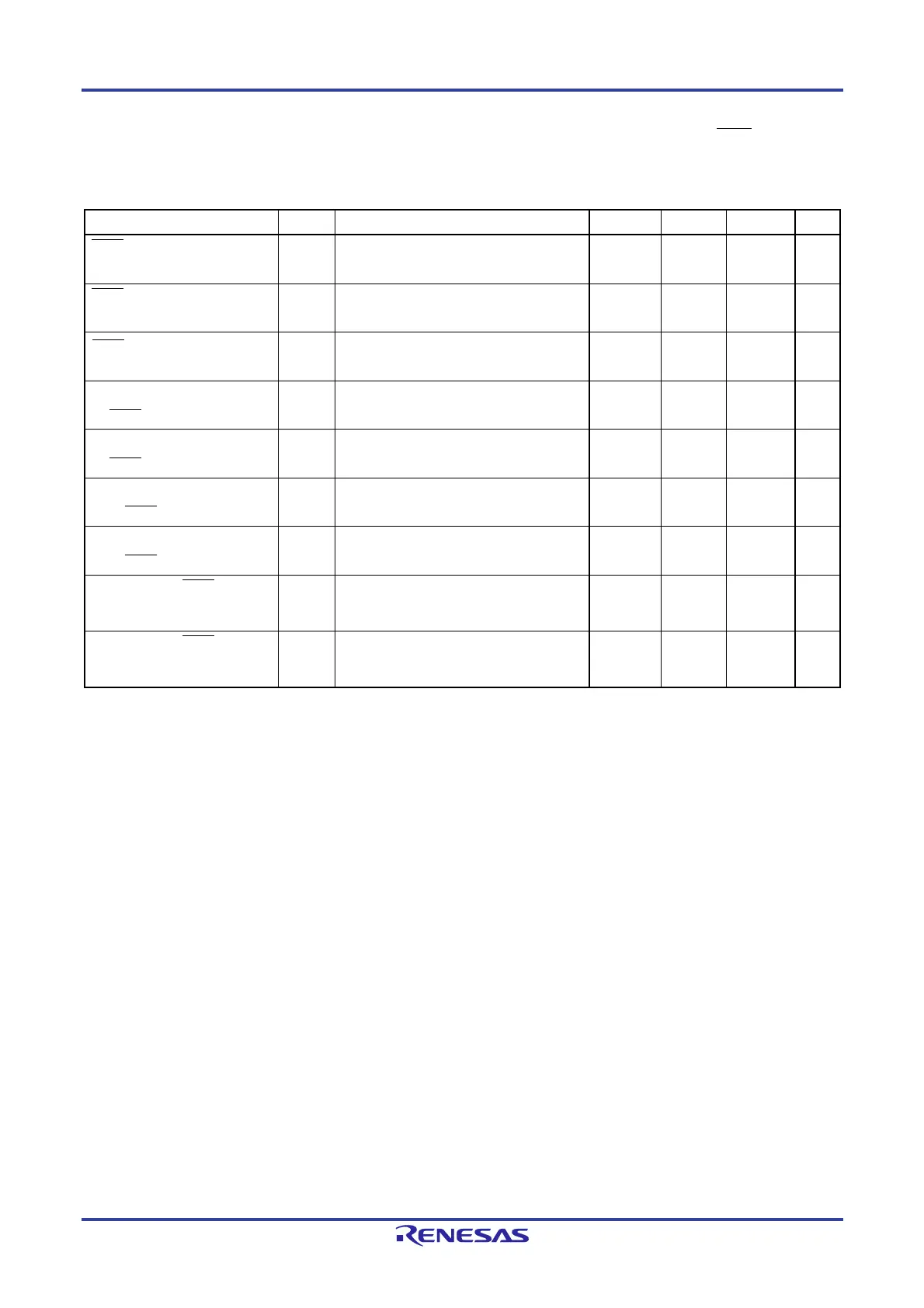
(9) During communication at different potential (3-V supply system) (CSI mode) (master mode, SCKp … internal
clock output, normal slew rate)
(TA = -40 to +105C, 4.0 V EVDD0 = EVDD1 = VDD 5.5 V, VSS = EVSS0 = EVSS1 = 0 V)
Parameter Symbol Conditions MIN. TYP. MAX. Unit
SCKp cycle time tKCY1
2.7 V V
b EVDD0,
C
b = 30 pF, Rb = 1.4 kΩ
400
Note3
ns
SCKp high-level width tKH1
2.7 V V
b EVDD0,
C
b = 30 pF, Rb = 1.4 kΩ
t
KCY1
/2 – 75
ns
SCKp low-level width tKL1
2.7 V V
b EVDD0,
C
b = 30 pF, Rb = 1.4 kΩ
t
KCY1
/2 – 20
ns
SIp setup time
(to SCKp)
Note 1
t
SIK1
2.7 V V
b EVDD0,
C
b = 30 pF, Rb = 1.4 kΩ
150 ns
SIp setup time
(to SCKp)
Note 2
t
SIK1
2.7 V V
b EVDD0,
C
b = 30 pF, Rb = 1.4 kΩ
70 ns
SIp hold time
(from SCKp)
Note 1
t
KSI1
2.7 V V
b EVDD0,
C
b = 30 pF, Rb = 1.4 kΩ
30 ns
SIp hold time
(from SCKp)
Note 2
t
KSI1
2.7 V V
b EVDD0,
C
b = 30 pF, Rb = 1.4 kΩ
30 ns
Delay time from SCKp to SOp
output
Note1
t
KSO1
2.7 V V
b EVDD0,
C
b = 30 pF, Rb = 1.4 kΩ
120 ns
Delay time from SCKp to SOp
output
Note2
t
KSO1
2.7 V V
b EVDD0,
C
b = 30 pF, Rb = 1.4 kΩ
40 ns
Notes 1. When DAPmn = 0 and CKPmn = 0, or DAPmn = 1 and CKPmn = 1.
2. When DAPmn = 0 and CKPmn = 1, or DAPmn = 1 and CKPmn = 0.
3. t
KCY1 4/fCLK must also be satisfied.
 Loading...


