RL78/F13, F14 CHAPTER 35 ELECTRICAL SPECIFICATIONS (GRADE K)
R01UH0368EJ0210 Rev.2.10 1766
Dec 10, 2015
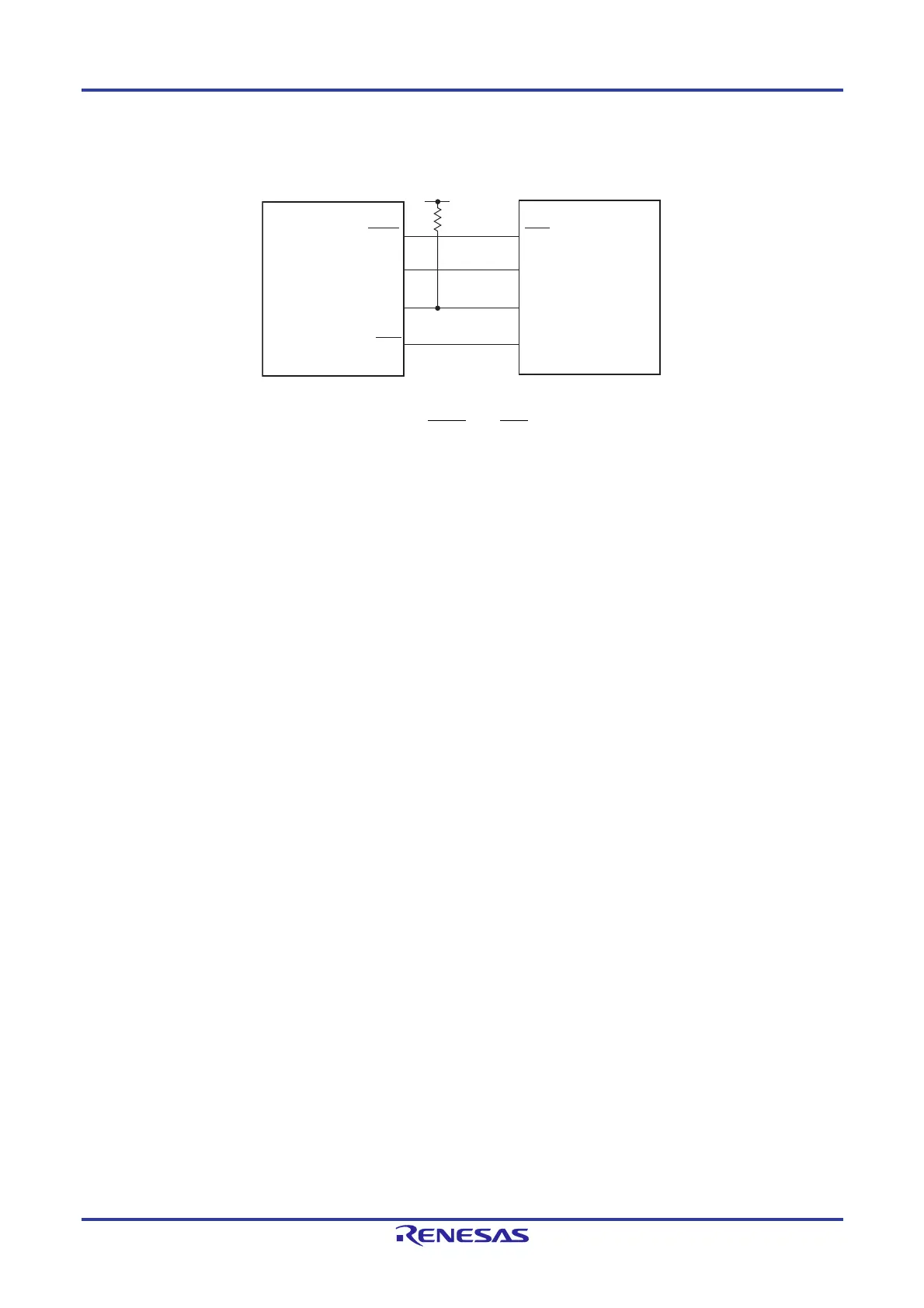
CSI mode connection diagram (during communication at different potential)
Caution Select the TTL input buffer for the SIp, SCKp and SSIp pins and N-ch open-drain output mode for the
SOp pin.
Remarks 1. Rb [Ω]: Communication line (SOp) pull-up resistance, Cb [F]: Communication line (SOp) load capacitance,
V
b [V]: Communication line voltage
2. p: CSIp (p = 00, 01, 10, 11), m: Unit m (m = 0, 1), n: Channel n (n = 0, 1)
3. AC characteristics of the serial array unit during communication at different potential in CSI mode are
measured with the
VIH and VIL below:
When 4.0 V EVDD0 5.5 V, 2.7 V Vb 4.0 V: VIH = 2.2 V, VIL = 0.8 V
SCKp
SOp
SCK
SI
SSIp
SSO
User's device
SIp SO
Vb
Rb
<Slave>
RL78
microcontroller

 Loading...


