EasyManuals Logo

Renesas RL78 Series User Manual

Renesas RL78 Series
1879 pages
To Next Page IconTo Next Page
To Previous Page IconTo Previous Page
Page #232 background imageLoading...
Page #232 background image
RL78/F13, F14 CHAPTER 3 CPU ARCHITECTURE
R01UH0368EJ0210 Rev.2.10 200
Dec 10, 2015
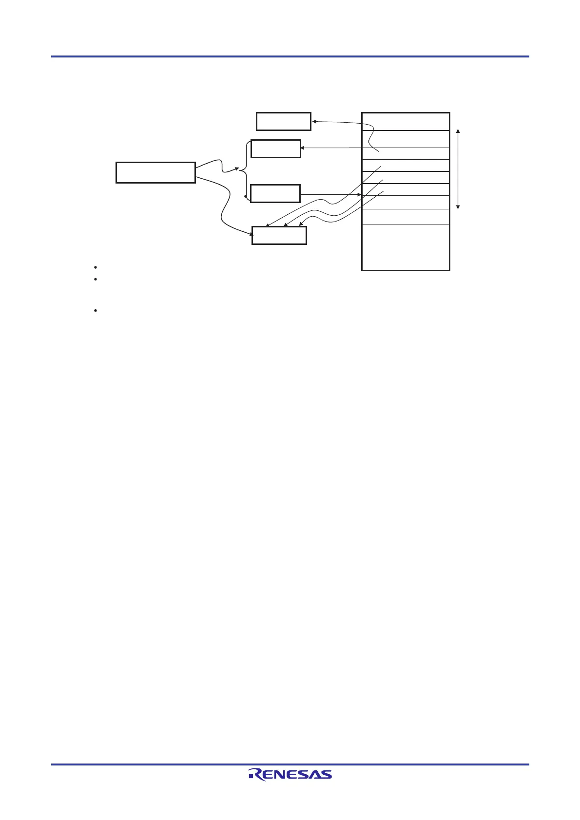
Figure 3-69. Example of RETI, RETB
RETI, RETB
SP
F0000H
PC
SP
PSW
Stack
area
Memory
SP+3 (SP+3)
(SP+2)
(SP+1)
(SP)
SP+2
SP+1
SP
SP+4
OP-code
<1>
<1>
Instruction code
<2>
<3>
Stack addressing is specified <1>.
The contents of addresses SP, SP + 1, SP + 2, and SP + 3 are
stored in PC bits 7 to 0, 15 to 8, 19 to 16, and the PSW, respectively
<2>.
The value of SP <3> is increased by four
.

Table of Contents

Other manuals for Renesas RL78 Series

Questions and Answers:

Question and Answer IconNeed help?

Do you have a question about the Renesas RL78 Series and is the answer not in the manual?

Renesas RL78 Series Specifications

General IconGeneral
CoreRL78
CPU Clock SpeedUp to 32 MHz
Flash MemoryUp to 512 KB
RAMUp to 32 KB
Operating Voltage1.6 V to 5.5 V
Low Power ModesHALT, STOP, SNOOZE
CPU Architecture16-bit
Temperature Range-40°C to +85°C
PackageLQFP
Timers16-bit timers
Communication InterfacesUART, I2C, LIN
A/D Converter12-bit

Related product manuals