RL78/F13, F14 CHAPTER 4 PORT FUNCTIONS
R01UH0368EJ0210 Rev.2.10 282
Dec 10, 2015
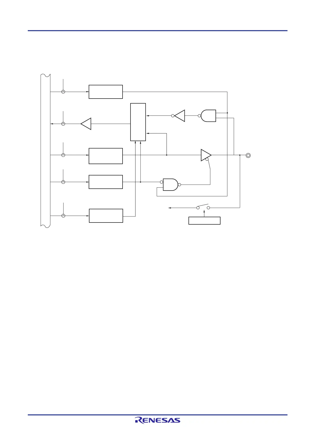
Figure 4-57 shows a block diagram of port 9 for 100-pin products.
Figure 4-57. Block Diagram of P90 to P97
P90/ANI10,
P91/ANI11,
P92/ANI12,
P93/ANI13,
P94/ANI14,
P95/ANI15,
P96/ANI16,
P97/ANI17
WR
ADPC
RD
WR
PORT
WR
PM
ADPC
PM9
P9
PM90 to PM97
P90 to P97
ADPC4 to ADPC0
WR
PMS
PMS
PMS0
0: Analog input
1: Digital I/O
Internal bus
Output latch
Selector
A/D converter
ADS
ADS4 to ADS0
P9: Port register 9
PM9: Port mode register 9
PMS: Port mode select register
ADPC: A/D port configuration register
ADS: Analog input channel specification register
RD: Read signal
WRxx: Write signal

 Loading...


