RL78/F13, F14 CHAPTER 5 CLOCK GENERATOR
R01UH0368EJ0210 Rev.2.10 384
Dec 10, 2015
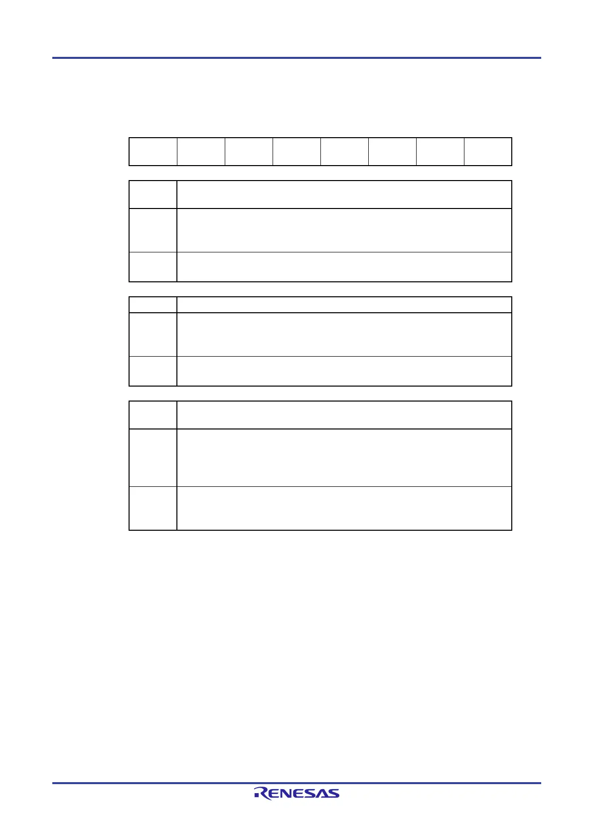
Figure 5-13. Format of Peripheral Enable Register 2 (PER2)
Address: F02C1H After reset: 00H R/W
Symbol 7 6 5 4 <3> <2> 1 <0>
PER2 0 0 0 0
LIN1EN
Note 1
LIN0EN 0
CAN0EN
Note 2
LIN1EN
Note 1
Control of LIN1 input clock supply
0 Stops input clock supply.
Disables writing to the SFR used by LIN1.
LIN1 is in the reset state.
1 Enables input clock supply.
Enables reading from and writing to the SFR used by LIN1.
LIN0EN Control of LIN0 input clock supply
0 Stops input clock supply.
Disables writing to the SFR used by LIN0.
LIN0 is in the reset state.
1 Enables input clock supply.
Enables reading from and writing to the SFR used by LIN0.
CAN0EN
Note 2
Control of CAN input clock supply/control of CANi wakeup interrupt
0 Stops input clock supply.
Disables writing to the SFR used by CAN.
CAN is in the reset state.
Disables CANi wakeup interrupt.
1 Enables input clock supply.
Enables reading from and writing to the SFR used by CAN.
Enables CANi wakeup interrupt.
Notes 1. Only in the RL78/F14 products with at least 128 Kbytes of code flash memory and the 100-
pin products of the RL78/F14.
2. Only in the RL78/F13 (CAN and LIN incorporated) and RL78/F14 products.
Caution Be sure to clear the following bits to 0.
Bits 0, 1, 3, 4, 5, 6, and 7 in the RL78/F13 (LIN incorporated) products
Bits 1, 3, 4, 5, 6, and 7 in the RL78/F13 (CAN and LIN incorporated) products and the
RL78/F14 products with 30, 32, 48, 64, or 80 pins and up to 96 Kbytes of code flash
memory
Bits 1, 4, 5, 6, and 7 in the RL78/F14 products with at least 128 Kbytes of code flash
memory and the 100-pin products of the RL78/F14

 Loading...


