RL78/F13, F14 CHAPTER 8 TIMER RD
R01UH0368EJ0210 Rev.2.10 634
Dec 10, 2015
Table 8-16. PWM Mode Specifications
Item Specification
Count sources
Note
fCLK, fPLL, fIH, fSUB, fIL
External signal input to the TRDCLK0 pin (active edge selected by a program)
Count operations Increment
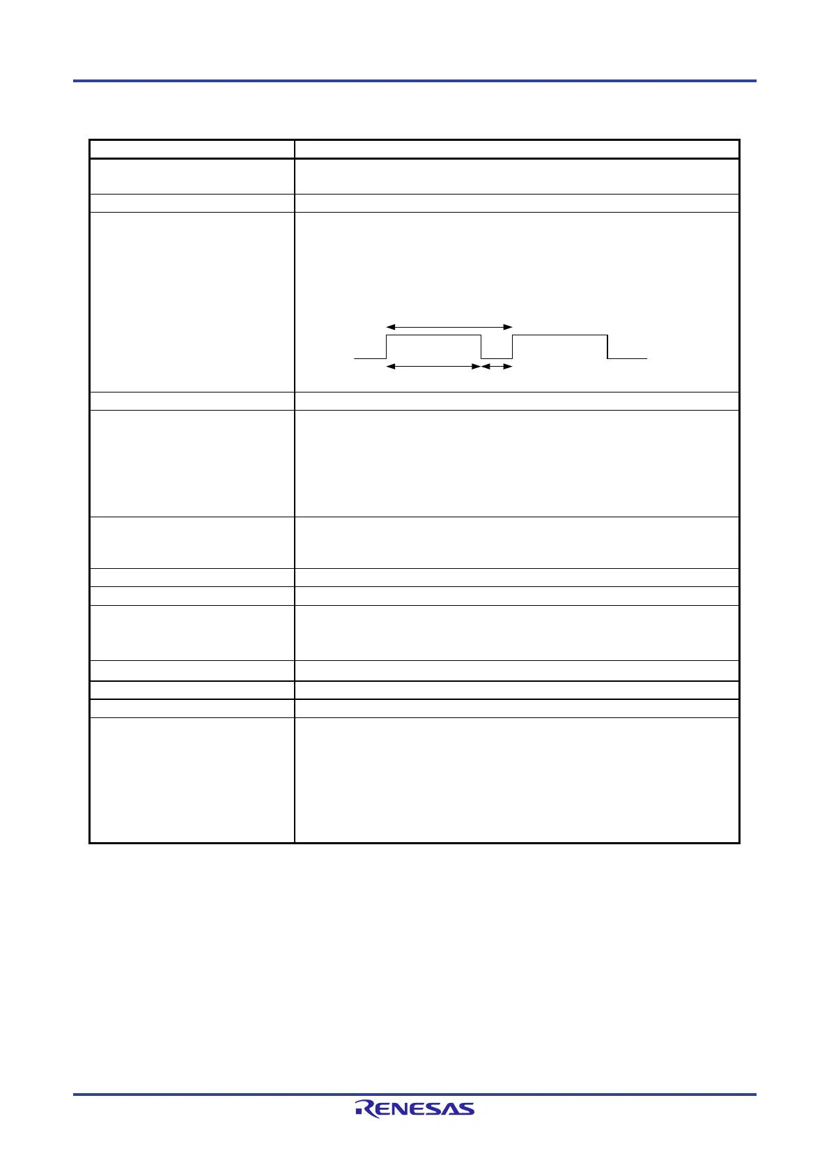
PWM waveform PWM period: 1/fk x (m + 1)
Active level width: 1/fk x (m - n)
Inactive level width: 1/fk x (n + 1)
fk: Frequency of count source
m: Value set in the TRDGRAi register
n: Value set in the TRDGRji register
Count start condition 1 (count starts) is written to the TSTARTi bit in the TRDSTR register.
Count stop conditions • 0 (count stops) is written to the TSTARTi bit in the TRDSTR register when the CSELi
bit in the TRDSTR register is set to 1.
The PWM output pin holds the output level before the count stops.
• When the CSELi bit in the TRDSTR register is set to 0, the count stops at the
compare match with the TRDGRAi register.
The PWM output pin holds the level after output change by compare match.
Interrupt request generation timing • Compare match (content of the TRDi register matches content of the TRDGRhi
register)
• TRDi register overflow
TRDIOA0 pin function I/O port or TRDCLK (external clock) input
TRDIOA1 pin function I/O port
TRDIOB0, TRDIOC0, TRDIOD0,
TRDIOB1, TRDIOC1, TRDIOD1
pin function
I/O port or pulse output (selectable for each pin)
INTP0 pin function
Pulse output forced cutoff signal input (port or INTP0 interrupt input)
Read from timer The count value can be read by reading the TRDi register.
Write to timer The value can be written to the TRDi register.
Selectable functions • One to three PWM output pins selectable with timer RDi
Either one pin or multiple pins of TRDIOBi, TRDIOCi, and TRDIODi.
• Active level selectable for each pin.
• Initial output level selectable for each pin.
• Synchronous operation (see 8. 3. 1 (3) Synchronous Operation)
• Buffer operation (see 8. 3. 1 (2) Buffer Operation)
• Pulse output forced cutoff signal input (see 8. 3. 1 (4) Pulse Output Forced Cutoff)
Note When selecting the count source for the timer RD, set the same clock source as the count source for fCLK before
setting bit 4 (TRD0EN) in the peripheral enable register 1 (PER1).
Remark i = 0 or 1, j = B, C, or D, h = A, B, C, or D
m + 1
n + 1 m - n (When low is selected as the active level)

 Loading...


