RL78/F13, F14 CHAPTER 8 TIMER RD
R01UH0368EJ0210 Rev.2.10 638
Dec 10, 2015
Table 8-17. Reset Synchronous PWM Mode Specifications
Item Specification
Count sources
Note
fCLK, fPLL, fIH, fSUB, fIL
External signal input to the TRDCLK0 pin (active edge selected by a program)
Count operations The TRD0 register is incremented (the TRD1 register is not used).
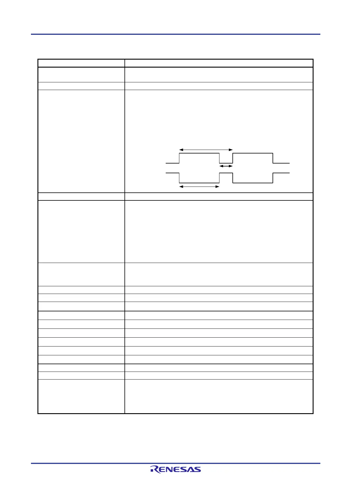
PWM waveform PWM period: 1/fk x (m + 1)
Active level of normal-phase: 1/fk x (m - n)
Inactive level of counter-phase: 1/fk x (n + 1)
fk: Frequency of count source
m: Value set in the TRDGRA0 register
n: Value set in the TRDGRB0 register (PWM1 output)
Value set in the TRDGRA1 register (PWM2 output)
Value set in the TRDGRB1 register (PWM3 output)
Count start condition 1 (count starts) is written to the TSTART0 bit in the TRDSTR register.
Count stop conditions
• 0 (count stops) is written to the TSTART0 bit when the CSEL0 bit in the TRDSTR
register is set to 1.
The PWM output pin outputs the initial output level selected by bits OLS0 and OLS1
in the TRDFCR register.
• When the CSEL0 bit in the TRDSTR register is set to 0, the count stops at the
compare match with the TRDGRA0 register.
The PWM output pin outputs the initial output level selected by bits OLS0 and OLS1
in the TRDFCR register.
Interrupt request generation timing
• Compare match (content of the TRD0 register matches content of registers
TRDGRj0, TRDGRA1, and TRDGRB1)
• TRD0 register overflow
TRDIOA0 pin function I/O port or TRDCLK (external clock) input
TRDIOB0 pin function PWM1 output normal-phase output
TRDIOD0 pin function
PWM1 output counter-phase output
TRDIOA1 pin function
PWM2 output normal-phase output
TRDIOC1 pin function
PWM2 output counter-phase output
TRDIOB1 pin function
PWM3 output normal-phase output
TRDIOD1 pin function
PWM3 output counter-phase output
TRDIOC0 pin function
Output inverted every PWM period
INTP0 pin function
Pulse output forced cutoff signal input (port or INTP0 interrupt input)
Read from timer The count value can be read by reading the TRD0 register.
Write to timer The value can be written to the TRD0 register.
Selectable functions
•The normal-phase and counter-phase active level and initial output level are selected
individually.
• Buffer operation (see 8. 3. 1 (2) Buffer Operation)
• Pulse output forced cutoff signal input (see 8. 3. 1 (4) Pulse Output Forced Cutoff)
Note When selecting the count source for the timer RD, set the same clock source as the count source for fCLK before
setting bit 4 (TRD0EN) in the peripheral enable register 1 (PER1).
Remark j = A, B, C, or D
m + 1
n + 1
m - n
(When low is selected as the active level)
Normal-phase
Counter-phase

 Loading...


