RL78/F13, F14 CHAPTER 2 PIN FUNCTIONS
R01UH0368EJ0210 Rev.2.10 67
Dec 10, 2015
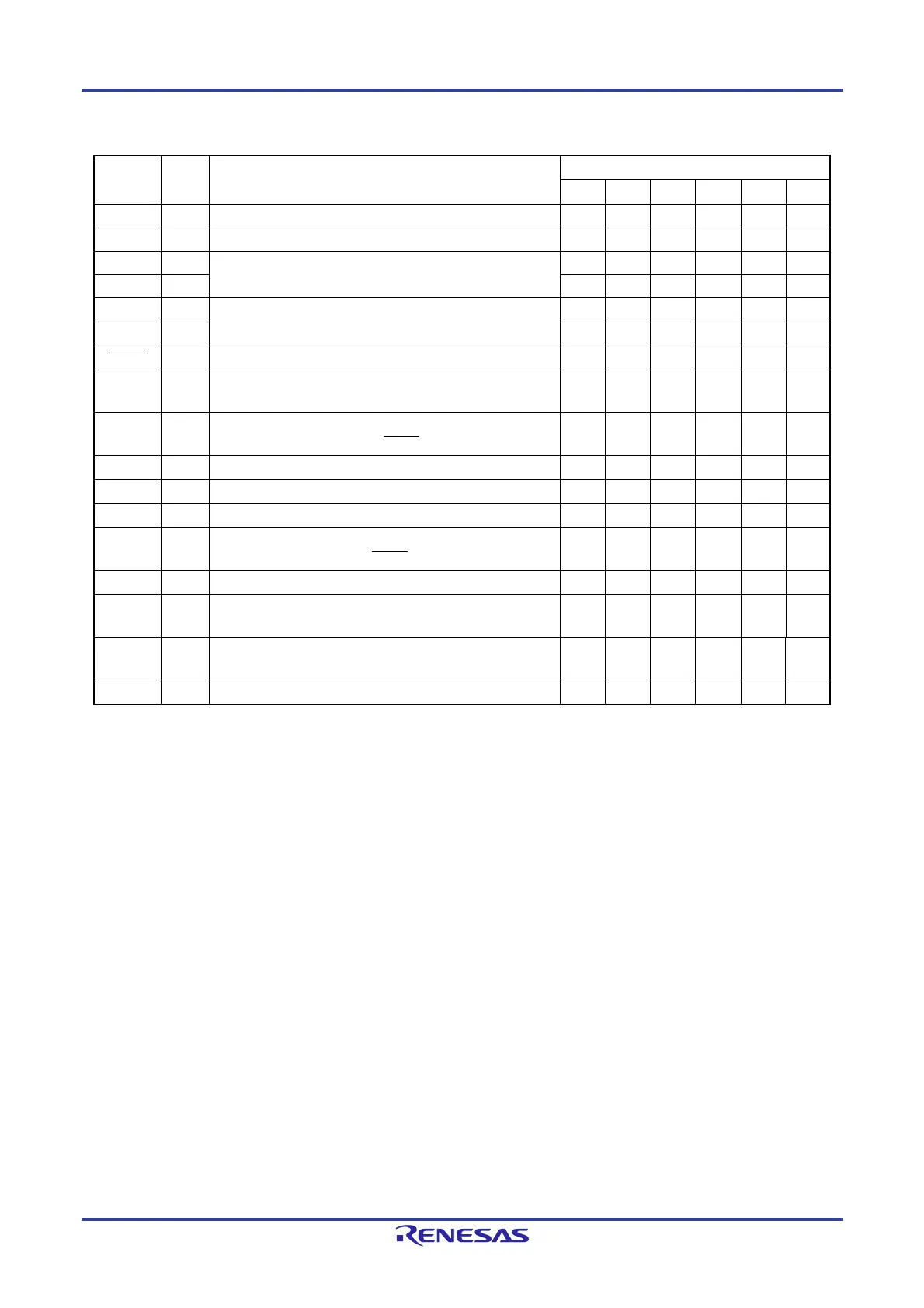
Table 2-4. List of RL78/F13 (LIN incorporated) Pins Other than Port Pins (4/4)
Pin
Function
I/O Function Pin Count
80-pin 64-pin 48-pin 32-pin 30-pin 20-pin
EXCLK Input External clock input for main system clock
EXCLKS Input External clock input for subsystem clock
X1 Resonator connection for main system clock
X2
XT1
Note
Resonator connection for subsystem clock
XT2
Note
RESET Input External reset input
REGC
Regulator output stabilization capacitance connection for internal
operation.
Connect to Vss via the capacitor (0.47 to 1 F).
VDD
Positive power supply for the P33, P34, P80 to P87, P90 to P97, P100
to P105, P121 to P124, P137, and RESET pins
EVDD0 Positive power supply for the pins that are not connected to VDD
AVREFP Input A/D converter reference voltage (+ side) input
AVREFM Input A/D converter reference voltage (- side) input
VSS
Ground potential for the P33, P34, P80 to P87, P90 to P97, P100 to
P105, P121 to P124, P137, and RESET pins
EVSS0 Ground potential for the pins that are not connected to VSS
TOOLRXD Input
UART reception pin for the external device connection used during flash
memory programming
TOOLTXD Output
UART transmission pin for the external device connection used during
flash memory programming
TOOL0 I/O Data input/output for flash memory programmer/debugger
Note Do not use the XT1 and XT2 pin functions in grade-Y products.

 Loading...


