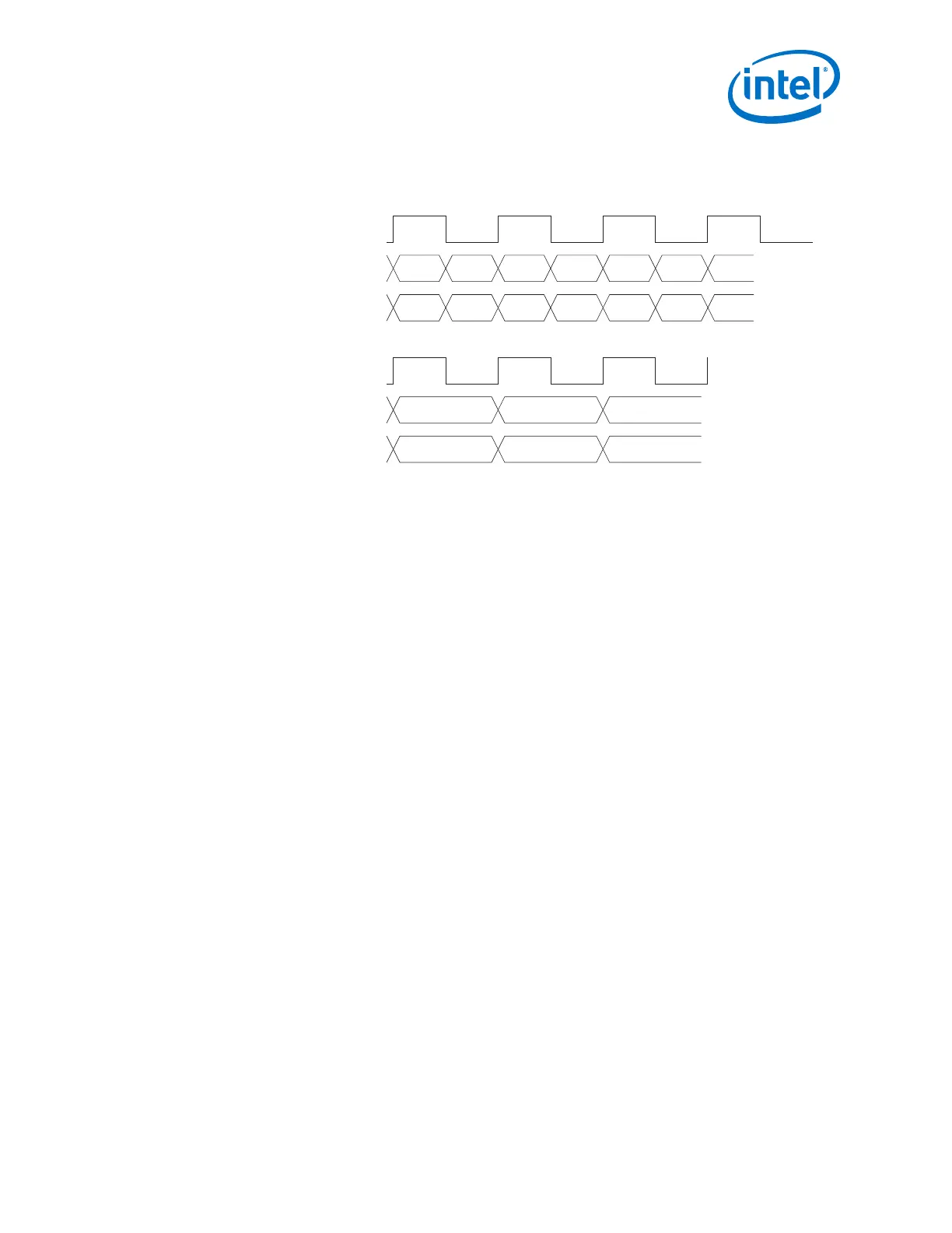
Figure 59. XGMII Interface (DDR) and Transceiver Interface (SDR) for 10GBASE-R
Configurations
D0TXD/RXD[31:0] D1 D2 D3 D4 D5 D6
C0TXC/RXC[3:0] C1 C2 C3 C4 C5 C6
{D1, D0} {D3, D2} {D5, D4}
{C1, C0}
TXD/RXD[63:0]
Interface Clock (156.25) MHz
Interface Clock (156.25) MHz
Transceiver Interface (SDR)
XGMII Transfer (DDR)
TXC/RXC[7:0] {C3, C2} {C5, C4}
Note: Clause 46 of the IEEE 802.3-2008 specification defines the XGMII interface between
the 10GBASE-R PCS and the Ethernet MAC/RS.
The dedicated reference clock input to the variants of the 10GBASE-R PHY can be run
at either 322.265625 MHz or 644.53125 MHz.
For 10GBASE-R, you must achieve 0 ppm of the frequency between the read clock of
TX phase compensation FIFO (PCS data) and the write clock of TX phase
compensation FIFO (XGMII data in the FPGA fabric). This can be achieved by using the
same reference clock as the transceiver dedicated reference clock input as well as the
reference clock input for a core PLL (fPLL, for example) to produce the XGMII clock.
The same core PLL can be used to drive the RX XGMII data. This is because the RX
clock compensation FIFO is able to handle the frequency PPM difference of ±100 ppm
between RX PCS data driven by the RX recovered clock and RX XGMII data.
Note: 10GBASE-R is the single-channel protocol that runs independently. Therefore Intel
recommends that you use the presets for selecting the suitable 10GBASE-R variants
directly. If it is being configured through the Native PHY IP, the channel bonding option
should be disabled. Enabling the channel bonding for multiple channels could degrade
the link performance in terms of TX jitter eye and RX jitter tolerance.
2.6.2.1.1. TX FIFO and RX FIFO
In 10GBASE-R configuration, the TX FIFO behaves as a phase compensation FIFO and
the RX FIFO behaves as a clock compensation FIFO.
In 10GBASE-R with 1588 configuration, both the TX FIFO and the RX FIFO are used in
register mode. The TX phase compensation FIFO and the RX clock compensation FIFO
are constructed in the FPGA fabric by the PHY IP automatically.
In 10GBASE-R with KR FEC configuration, you use the TX FIFO in phase compensation
mode and the RX FIFO behaves as a clock compensation FIFO.
Related Information
Arria 10 Enhanced PCS Architecture on page 461
For more information about the Enhanced PCS Architecture
2. Implementing Protocols in Arria 10 Transceivers
UG-01143 | 2018.06.15
Intel
®
Arria
®
10 Transceiver PHY User Guide
129