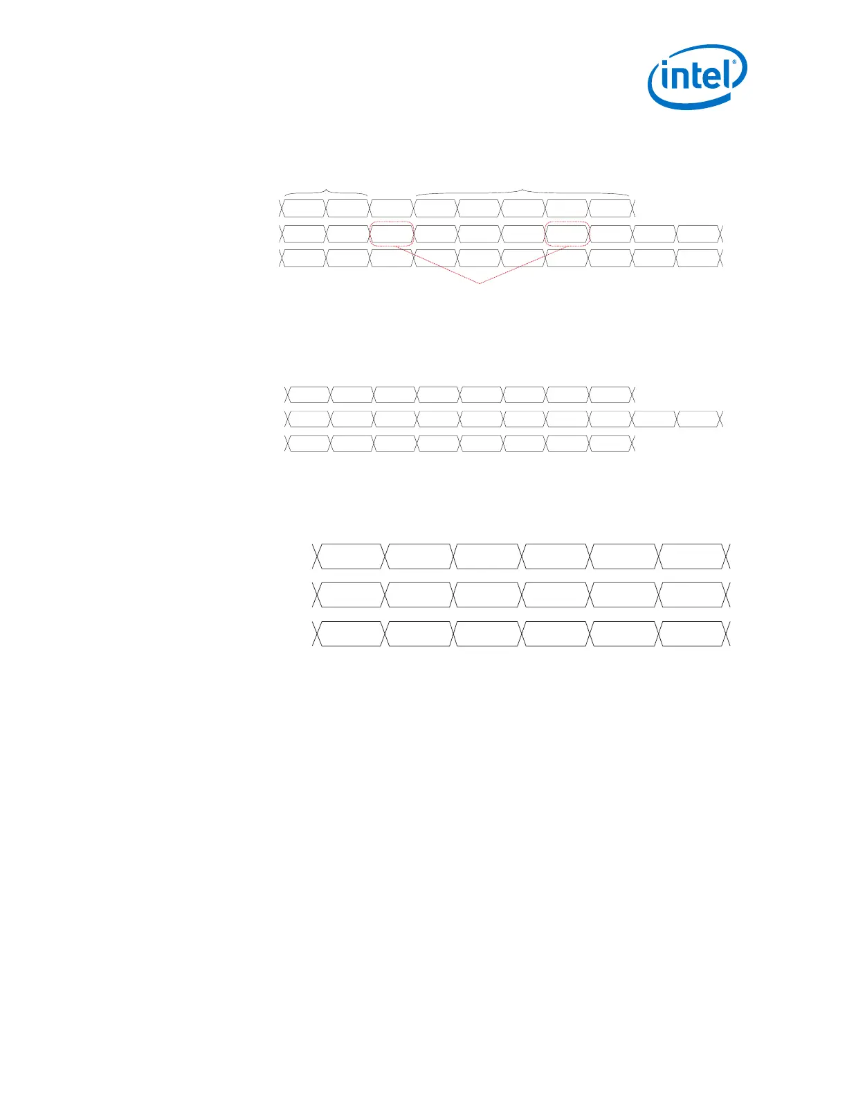
Figure 93. Rate Match Insertion
The figure below shows an example of rate match insertion in the case where two SKP symbols must be
inserted. Only one /K28.0/ SKP symbol is inserted per SKP ordered set received.
rmfifo_input_data
rx_parallel_data
First SKP Ordered Set
Second SKP Ordered Set
SKP Symbol Inserted
K28.5 K28.0 Dx.y K28.5 K28.0 K28.0 K28.0 K28.0
K28.5 K28.0 K28.0 Dx.y K28.5 K28.0
K28.0 K28.0 K28.0 K28.0
pipe_rx_status[2:0]
3’b001 xxx xxx xxx 3’b001 xxx
xxx xxx xxx xxx
Figure 94. Rate Match FIFO Full
The rate match FIFO in PIPE mode automatically deletes the data byte that causes the FIFO to go full and
drives pipe_rx_status[2:0] = 3'b101 synchronous to the subsequent data byte. The figure below shows
the rate match FIFO full condition in PIPE mode. The rate match FIFO becomes full after receiving data byte
D4.
D1 D2 D3 D4 D5 D6 D7 D8
D1 D2 D3 D4 D8 xx xx xxD6
D7
tx_parallel_data
rx_parallel_data
pipe_rx_status[2:0] xxx xxx xxx xxx 3’b101 xxx xxx xxx
Figure 95. Rate Match FIFO Empty
The rate match FIFO automatically inserts /K30.7/ (9'h1FE) after the data byte that causes the FIFO to become
empty and drives pipe_rx_status[2:0] = 3'b110 synchronous to the inserted /K30.7/ (9'h1FE). The figure
below shows rate match FIFO empty condition in PIPE mode. The rate match FIFO becomes empty after
reading out data byte D3.
D1 D2 D3 D4 D5 D6
D1 D2 D3 /K.30.7/ D4
D5
tx_parallel_data
rx_parallel_data
pipe_rx_status[2:0] xxx xxx xxx 3’b110 xxx
xxx
PIPE 0 ppm
The PIPE mode also has a "0 ppm" configuration option that can be used in
synchronous systems. The Rate Match FIFO Block is not expected to do any clock
compensation in this configuration, but latency is minimized.
2.7.2.1.8. PCIe Reverse Parallel Loopback
PCIe reverse parallel loopback is only available in a PCIe functional configuration for
Gen1, Gen2, and Gen3 data rates. The received serial data passes through the
receiver CDR, deserializer, word aligner, and rate matching FIFO buffer. The data is
then looped back to the transmitter serializer and transmitted out through the
transmitter buffer. The received data is also available to the FPGA fabric through the
rx_parallel_data port. This loopback mode is based on PCIe specification 2.0.
Arria 10 devices provide an input signal pipe_tx_detectrx_loopback to enable
this loopback mode.
Note:
This is the only loopback option supported in PIPE configurations.
2. Implementing Protocols in Arria 10 Transceivers
UG-01143 | 2018.06.15
Intel
®
Arria
®
10 Transceiver PHY User Guide
235