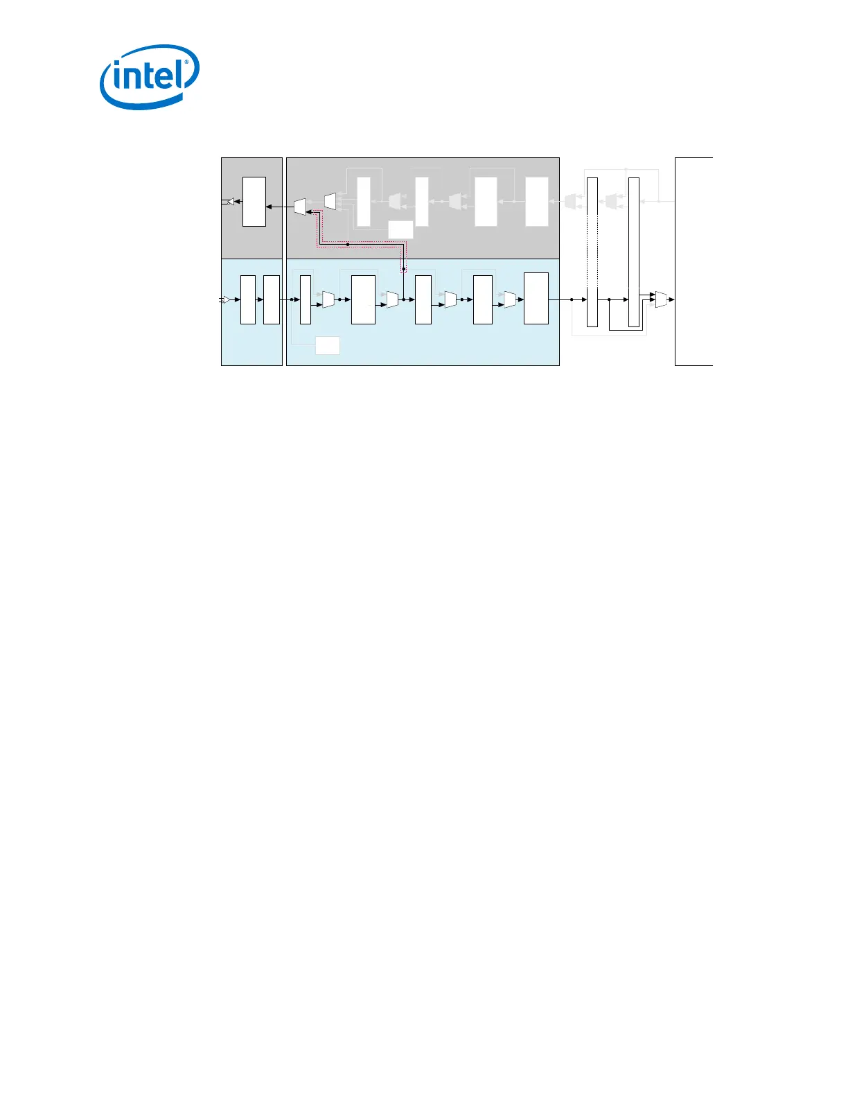
Figure 96. PCIe Reverse Parallel Loopback Mode Datapath
PCI Express Hard IP
PIPE Interface
RX
FIFO
Byte
Deserializer
8B/10B Decoder
Rate Match FIFO
Receiver PMA
Word Aligner
Deserializer
CDR
Receiver Standard PCS
Transmitter Standard PCS
Transmitter PMA
Serializer
tx_serial_data rx_serial_data
FPGA
Fabric
TX TX
FIFOFIFO
Byte SerializerByte Serializer
8B/10B Encoder8B/10B Encoder
PRBS
Generator
TX Bit Slip
PRBS
Reverse Parallel
Loopback Path
Verifier
Related Information
• Arria 10 Standard PCS Architecture on page 479
• Intel PHY Interface for the PCI Express* (PIPE) Architecture PCI Express 2.0
2.7.2.2. Gen3 Features
The following subsections describes the Arria 10 transceiver block support for PIPE
Gen3 features.
The PCS supports the PIPE 3.0 base specification. The 32-bit wide PIPE 3.0-based
interface controls PHY functions such as transmission of electrical idle, receiver
detection, and speed negotiation and control.
2.7.2.2.1. Auto-Speed Negotiation
PIPE Gen3 mode enables ASN between Gen1 (2.5 Gbps), Gen2 (5.0 Gbps), and Gen3
(8.0 Gbps) signaling data rates. The signaling rate switch is accomplished through
frequency scaling and configuration of the PMA and PCS blocks using a fixed 32-bit
wide PIPE 3.0-based interface.
The PMA switches clocks between Gen1, Gen2, and Gen3 data rates. For a non bonded
x1 channel, an ASN module facilitates speed negotiation in that channel. For bonded
x2, x4, x8 and x16 channels, the ASN module selects the master channel to control
the rate switch. The master channel distributes the speed change request to the other
PMA and PCS channels.
The PCIe Gen3 speed negotiation process is initiated when Hard IP or the FPGA fabric
requests a rate change. The ASN then places the PCS in reset, and dynamically shuts
down the clock paths to disengage the current active state PCS (either Standard PCS
or Gen3 PCS). If a switch to or from Gen3 is requested, the ASN automatically selects
the correct PCS clock paths and datapath selection in the multiplexers. The ASN block
then sends a request to the PMA block to switch the data rate, and waits for a rate
change done signal for confirmation. When the PMA completes the rate change and
sends confirmation to the ASN block, the ASN enables the clock paths to engage the
new PCS block and releases the PCS reset. Assertion of the pipe_phy_status signal
by the ASN block indicates the successful completion of this process.
2. Implementing Protocols in Arria 10 Transceivers
UG-01143 | 2018.06.15
Intel
®
Arria
®
10 Transceiver PHY User Guide
236