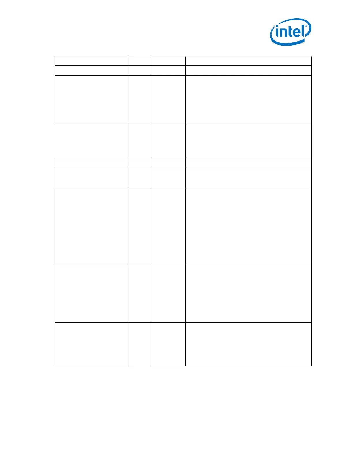
Port Direction Clock Domain Description
pll_locked
Output Asynchronous Active high status signal which indicates if PLL is locked.
pll_pcie_clk
Output N/A This is the hclk required for PIPE interface.
For Gen1x1, x2, x4, x8 use this port to drive the hclk for
the PIPE interface.
For Gen2x1, x2, x4, x8 use this port to drive the hclk for
the PIPE interface.
For Gen3x1, x2, x4, x8, use the pll_pcie_clk from fPLL
(configured as Gen1/Gen2) as the hclk for the PIPE
interface.
Pll_cal_busy
Output Asynchronous Status signal which is asserted high when PLL calibration is
in progress.
If this port is not enabled in Transceiver PHY Reset
Controller, then perform logical OR with this signal and the
tx_cal_busy output signal from Native PHY to input the
tx_cal_busy on the reset controller IP.
Mcgb_rst
Input Asynchronous Master CGB reset control.
mcgb_aux_clk0
Input N/A Used for Gen3 to switch between fPLL/ATX PLL during link
speed negotiation. For gen3x2, x4, x8 use the
mcgb_aux_clk input port on the ATX PLL.
tx_bonding_clocks[6n-1:0]]
Output N/A Optional 6-bit bus which carries the low speed parallel
clock outputs from the Master CGB. It is used for channel
bonding, and represents the x6/xN clock network.
For Gen1x1, this port is disabled.
For Gen1x2, x4, x8 connect the output from this port to
the tx_bonding_clocks input on Native PHY.
For Gen2x1, this port is disabled.
For Gen2x2, x4, x8 connect the output from this port to
the tx_bonding_clocks input on Native PHY.
For Gen3x1, this port is disabled.
For Gen3x2, x4, x8, use the tx_bonding_clocks output
from the ATX PLL to connect to the tx_bonding_clocks
input of the Native PHY.
pcie_sw[1:0]
Input Asynchronous 2-bit rate switch control input used for PCIe protocol
implementation.
For Gen1, this port is N/A
For Gen 2x2, x4, x8 connect the pipe_sw output from
Native PHY to this port.
For Gen3x2, x4, x8 connect the pipe_sw output from the
Native PHY to this port.
For Gen3x2, x4, x8, this port is not used. You must use the
pipe_sw from Native PHY to drive the pcie_sw input port
on the ATX PLL.
pcie_sw_done[1:0]
Output Asynchronous 2-bit rate switch status output used for PCIe protocol
implementation.
For Gen1, this port is N/A.
For Gen 2x2, x4, x8 connect the pcie_sw_done output
from ATX PLL to the pipe_sw_done input of Native PHY .
For Gen3x2, x4, x8 connect the pcie_sw_done output
from ATX PLL to the pipe_sw_done input of Native PHY.
Related Information
Using the Arria 10 Transceiver Native PHY IP Core on page 45
2. Implementing Protocols in Arria 10 Transceivers
UG-01143 | 2018.06.15
Intel
®
Arria
®
10 Transceiver PHY User Guide
265