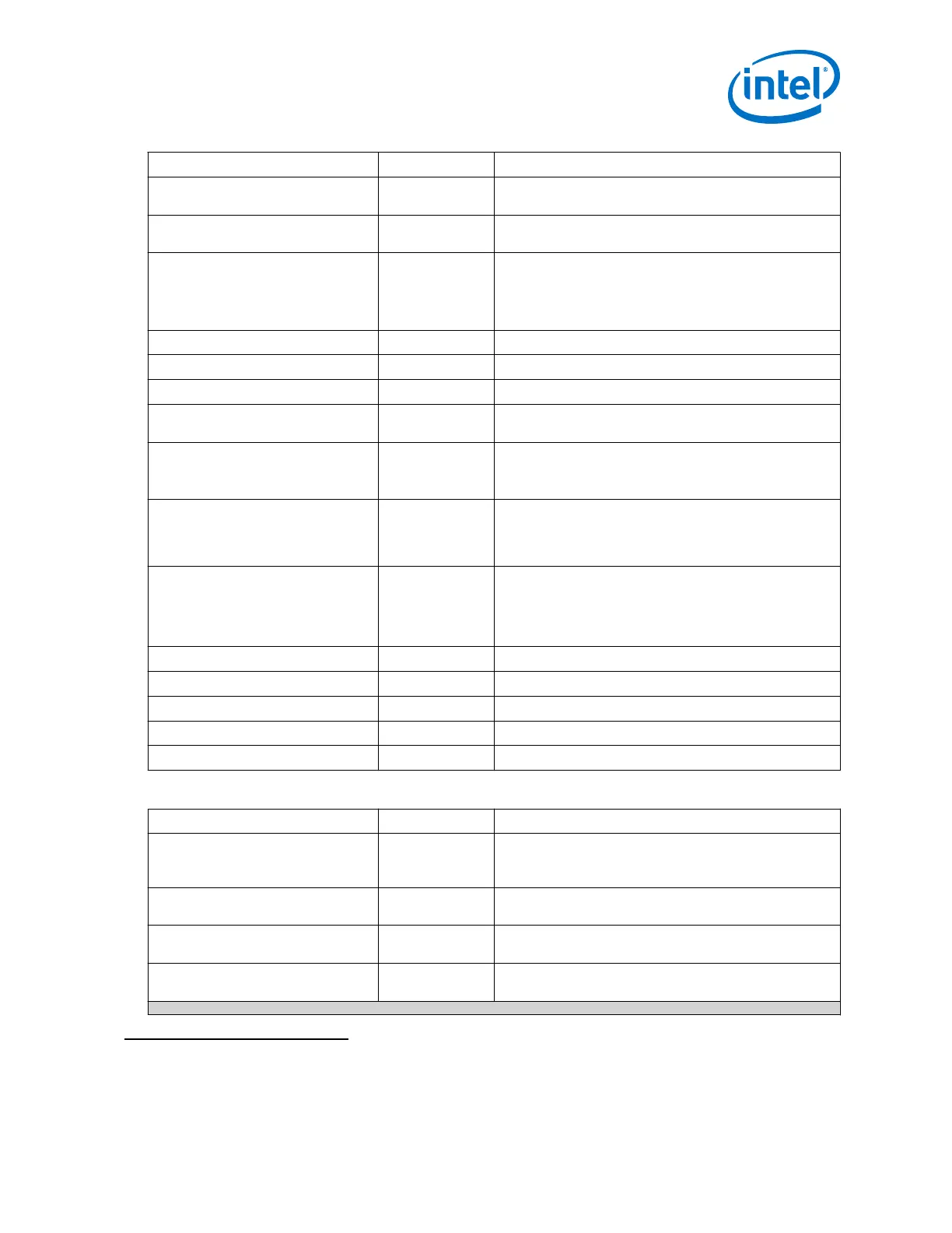
Parameters Range Description
This enables the PLL to output frequencies which are not
integral multiples of the input reference clock.
Enable physical output clock
parameters
On/Off Selecting this option allows you to manually specify M, N, C
and L counter values.
Enable clklow and fref ports
(56)
On/Off Enables fref and clklow clock ports for external lock
detector. In Transceiver mode when "enable fractional
mode" and "SDI_direct" prot_mode are selected,
pll_locked port is not available and user can create
external lock detector using fref and clklow clock ports.
Desired Reference clock frequency Refer to the GUI Specifies the desired PLL input reference clock frequency.
Actual reference clock frequency Read-only Displays the actual PLL input reference clock frequency.
Number of PLL reference clocks 1 to 5 Specify the number of input reference clocks for the fPLL.
New parameter: Selected reference
clock source
0 to 4 Specifies the initially selected reference clock input to the
fPLL.
Bandwidth Low
Medium
High
Specifies the VCO bandwidth.
Higher bandwidth reduces PLL lock time, at the expense of
decreased jitter rejection.
Operation mode Direct
Feedback
compensation
bonding
Specifies the feedback operation mode for the fPLL.
Multiply factor (M-counter) 8 to 127
(integer mode)
11 to 123
(fractional
mode)
Specifies the multiply factor (M-counter).
Divide factor (N-counter) 1 to 31 Specifies the divide factor (N-counter).
Divide factor (L-counter) 1, 2, 4, 8 Specifies the divide factor (L-counter).
Divide factor (K-counter) User defined Specifies the divide factor (K-counter).
PLL output frequency Read-only Displays the target output frequency for the PLL.
PLL Datarate Read-only Displays the PLL datarate.
Table 235. fPLL—Master Clock Generation Block Parameters and Settings
Parameters Range Description
Include Master Clock Generation
Block
On/Off When enabled, includes a master CGB as a part of the fPLL
IP core. The PLL output drives the master CGB.
This is used for x6/xN bonded and non-bonded modes.
Clock division factor 1, 2, 4, 8 Divides the master CGB clock input before generating
bonding clocks.
Enable x6/xN non-bonded high-
speed clock output port
On/Off Enables the master CGB serial clock output port used for
x6/xN non-bonded modes.
Enable PCIe clock switch interface On/Off Enables the control signals used for PCIe clock switch
circuitry.
continued...
(56)
The fPLL fref and clklow signals should only be used with the Intel external soft lock
detection logic.
3. PLLs and Clock Networks
UG-01143 | 2018.06.15
Intel
®
Arria
®
10 Transceiver PHY User Guide
363