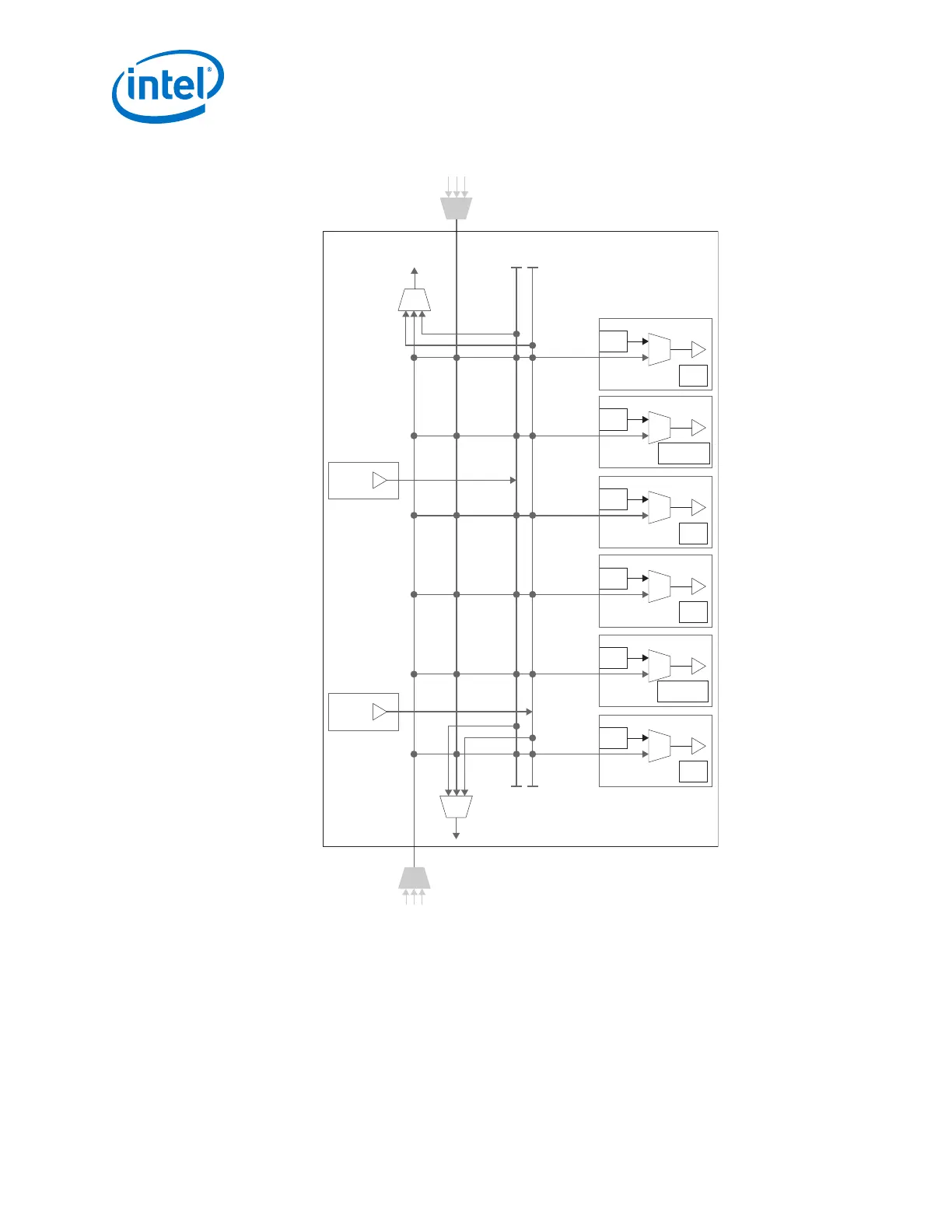
Figure 177. xN Clock Network
CGB
Ch 4
CDR
CGB
Ch 3
CDR
CGB
Ch 2
CGB
Ch 1
CDR
CGB
Ch 0
CDR
CGB
Ch 5
x6
Top
Master
CGB1
Master
CGB0
xN Up xN Down
x6
Bottom
xN Up
xN Down
CMU or CDR
CMU or CDR
The maximum channel span of a xN clock network is two transceiver banks above and
two transceiver banks below the bank that contains the driving PLL and the master
CGB. A maximum of 30 channels can be used in a single bonded or non-bonded xN
group.
The maximum data rate supported by the xN clock network while driving channels in
either the bonded or non-bonded mode depends on the voltage used to drive the
transceiver banks.
3. PLLs and Clock Networks
UG-01143 | 2018.06.15
Intel
®
Arria
®
10 Transceiver PHY User Guide
380