•
In this case, the PLL IP core has tx_bonding_clocks output bus with width
[5:0].
•
The Native PHY IP core has tx_bonding_clocks input bus with width [5:0]
multiplied by the number of transceiver channels (10 in this case). For 10
channels, the bus width is [59:0].
Note:
While connecting tx_bonding_clocks, leave tx_serial_clk open
to avoid any Intel Quartus Prime software fitter errors.
• Connect the PLL IP core to the PHY IP core by duplicating the output of the
PLL[5:0] for the number of channels. For 10 channels, the Verilog syntax for
the input port connection is .tx_bonding_clocks
({10{tx_bonding_clocks_output}}) .
Note: Although the above diagram looks similar to the 10-channel non-bonded configuration
example, the clock input ports on the transceiver channels bypass the local CGB in
x6/xN bonding configuration. This internal connection is taken care of when the
Native PHY channel bonding mode is set to Bonded.
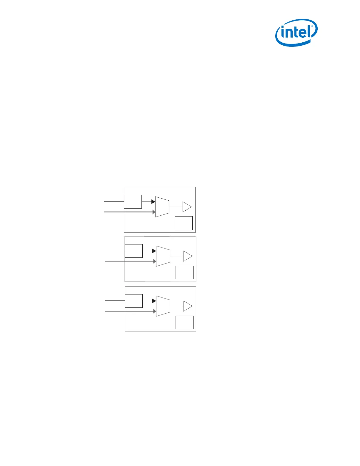
Figure 195. x6/xN Bonding Mode —Internal Channel Connections
CDR
CGB
Ch 0
CDR
CGB
Ch 1
CDR
CGB
Ch 2
(1)
Note: (1) The local CGB is bypassed by the clock input ports in bonded mode.
(1)
(1)
Related Information
xN Clock Lines on page 379
Information on xN Clock Network Span.
3.11.2.2. Implementing PLL Feedback Compensation Bonding Mode
In this bonding mode, the channel span limitations of xN bonding mode are removed.
This is achieved by dividing all channels into multiple bonding groups.
3. PLLs and Clock Networks
UG-01143 | 2018.06.15
Intel
®
Arria
®
10 Transceiver PHY User Guide
405