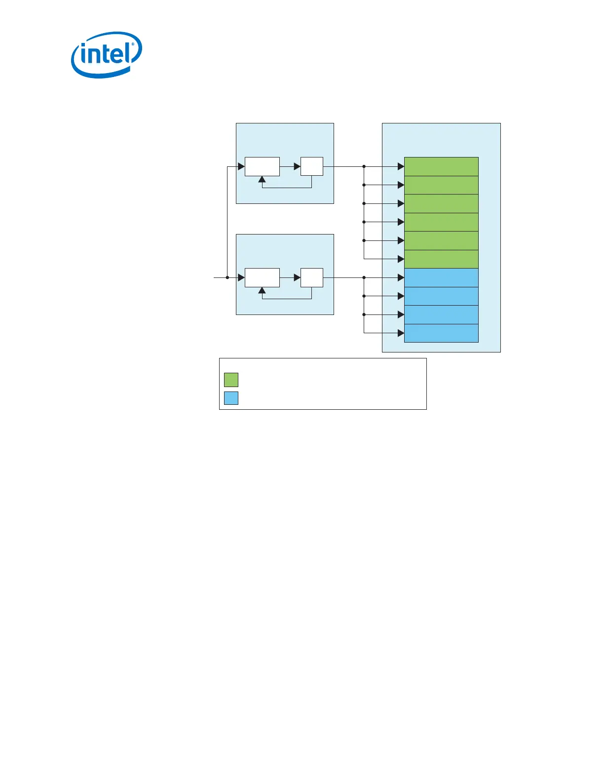
Figure 196. PHY IP Core and PLL IP Core Connection for PLL Feedback Compensation
Bonding
Transceiver PLL
Instance (5 GHz)
fPLL
Native PHY Instance
(10 CH Bonded 10 Gbps)
TX Channel
TX Channel
TX Channel
TX Channel
TX Channel
TX Channel
TX Channel
TX Channel
TX Channel
TX Channel
CGB
x6
x6
Feedback Clock
Transceiver PLL
Instance (5 GHz)
fPLL CGB
Feedback Clock
Legend:
TX channels placed in the adjacent transceiver bank.
TX channels placed in the same transceiver bank.
Reference clock
The data rate is limited by the x6 network speed limit. A disadvantage of using PLL
feedback compensation bonding is that it consumes more PLL resources. Each
transceiver bank consumes one PLL and one master CGB.
In PLL feedback compensation bonding mode, the N counter (reference clock divider)
is bypassed in order to ensure that the reference clock skew is minimized between the
PLLs in the bonded group. Because the N counter is bypassed, the PLL reference clock
has a fixed value for any given data rate.
The PLL IP Core Parameter Editor window displays the required data rate in the
PLL reference clock frequency drop down menu.
Steps to implement a PLL Feedback Compensation Bonding Configuration
1. Instantiate the PLL IP core (ATX PLL or fPLL) you want to use in your design. Refer
to Instantiating the ATX PLL IP Core on page 354 or Instantiating the fPLL IP Core
on page 362 for detailed steps. Because the CMU PLL cannot drive the master
CGB, only the ATX PLL or fPLL can be used for feedback compensation bonding.
2. Configure the PLL IP core using the IP Parameter Editor.
3. PLLs and Clock Networks
UG-01143 | 2018.06.15
Intel
®
Arria
®
10 Transceiver PHY User Guide
406