RL78/F13, F14 CHAPTER 16 SERIAL INTERFACE IICA
R01UH0368EJ0210 Rev.2.10 1025
Dec 10, 2015
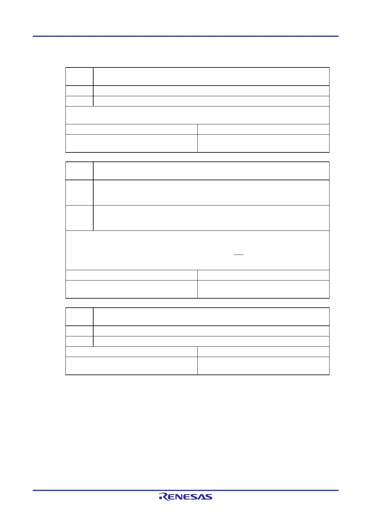
Figure 16-6. Format of IICA Control Register 00 (IICCTL00) (2/4)
SPIE0
Note 1
Enable/disable generation of interrupt request when stop condition is detected
0 Disable
1 Enable
If the WUP0 bit of IICA control register 01 (IICCTL01) is 1, no stop condition interrupt will be generated even if SPIE0
= 1.
Condition for clearing (SPIE0 = 0) Condition for setting (SPIE0 = 1)
Cleared by instruction
Reset
Set by instruction
WTIM0
Note 1
Control of wait and interrupt request generation
0 Interrupt request is generated at the eighth clock’s falling edge.
Master mode: After output of eight clocks, clock output is set to low level and wait is set.
Slave mode: After input of eight clocks, the clock is set to low level and wait is set for master device.
1 Interrupt request is generated at the ninth clock’s falling edge.
Master mode: After output of nine clocks, clock output is set to low level and wait is set.
Slave mode: After input of nine clocks, the clock is set to low level and wait is set for master device.
An interrupt is generated at the falling edge of the ninth clock during address transfer independently of the setting of
this bit. The setting of this bit is valid when the address transfer is completed. When in master mode, a wait is inserted
at the falling edge of the ninth clock during address transfers. For a slave device that has received a local address, a
wait is inserted at the falling edge of the ninth clock after an acknowledge (ACK) is issued. However, when the slave
device has received an extension code, a wait is inserted at the falling edge of the eighth clock.
Condition for clearing (WTIM0 = 0) Condition for setting (WTIM0 = 1)
Cleared by instruction
Reset
Set by instruction
ACKE0
Notes 1, 2
Acknowledgment control
0 Disable acknowledgment.
1 Enable acknowledgment. During the ninth clock period, the SDAA0 line is set to low level.
Condition for clearing (ACKE0 = 0) Condition for setting (ACKE0 = 1)
Cleared by instruction
Reset
Set by instruction
Notes 1. The signal of this bit is invalid while IICE0 is 0. Set this bit during that period.
2. The set value is invalid during address transfer and if the code is not an extension code.
When the device serves as a slave and the addresses match, an acknowledgment is generated
regardless of the set value.

 Loading...


