RL78/F13, F14 CHAPTER 36 ELECTRICAL SPECIFICATIONS (GRADE Y)
R01UH0368EJ0210 Rev.2.10 1825
Dec 10, 2015
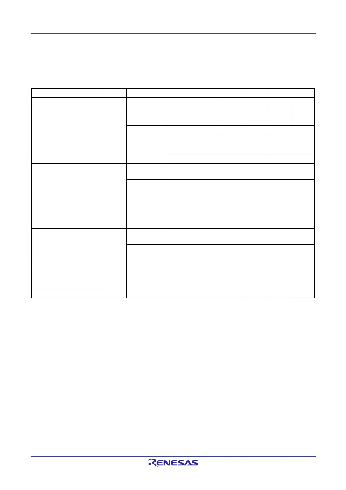
(3) When AVREF (+) = VDD (ADREFP1 = 0, ADREFP0 = 0), AVREF (-) = VSS (ADREFM = 0), target ANI pin: ANI0 to
ANI23, ANI24 to ANI30
(TA = -40 to +150C, 2.7 V EVDD0 = EVDD1 = VDD 5.5 V, VSS = EVSS0 = EVSS1 = 0 V, Reference voltage (+) = VDD,
Reference voltage (-) = V
SS)
Parameter Symbol Conditions MIN. TYP. MAX. Unit
Resolution RES 8 10 bit
Overall error
Note 1
AINL
10-bit resolution
ANI0 to ANI23
4.0 V VDD 5.5 V 1.2 5.0 LSB
2.7 V VDD < 4.0 V 1.2 5.5 LSB
10-bit resolution
ANI24 to ANI30
4.0 V V
DD 5.5 V 1.2 6.5 LSB
2.7 V VDD < 4.0 V 1.2 7.0 LSB
Conversion time tCONV 10-bit resolution 4.0 V VDD 5.5 V 2.125 39
µs
2.7 V VDD < 4.0 V 3.1875 39
µs
Zero-scale error
Notes 1, 2
EZS
10-bit resolution
ANI0 to ANI23
2.7 V V
DD 5.5 V 0.50 %FSR
10-bit resolution
ANI24 to ANI30
2.7 V V
DD 5.5 V 0.60 %FSR
Full-scale error
Notes 1, 2
EFS
10-bit resolution
ANI0 to ANI23
2.7 V VDD 5.5 V 0.50 %FSR
10-bit resolution
ANI24 to ANI30
2.7 V V
DD 5.5 V 0.60 %FSR
Integral linearity error
Note 1
ILE
10-bit resolution
ANI0 to ANI23
2.7 V VDD 5.5 V 3.5 LSB
10-bit resolution
ANI24 to ANI30
2.7 V V
DD 5.5 V 4.0 LSB
Differential linearity error
Note 1
DLE 10-bit resolution 2.7 V VDD 5.5 V 2.0 LSB
Analog input voltage VAIN ANI0 to ANI23
Note 3
0 VDD V
ANI24 to ANI30
Note 3
EVSS EVDD0 V
Internal reference voltage (+) VBGR 2.7 V VDD 5.5 V 1.38 1.45 1.52 V
Notes 1. Excludes quantization error (1/2 LSB).
2. This value is indicated as a ratio (%FSR) to the full-scale value.
3. The number of pins depends on the product. For details, refer to 2.1 Pin Function List.

 Loading...


