EasyManuals Logo

Renesas RL78 Series User Manual

Renesas RL78 Series
1879 pages
To Next Page IconTo Next Page
To Previous Page IconTo Previous Page
Page #305 background imageLoading...
Page #305 background image
RL78/F13, F14 CHAPTER 4 PORT FUNCTIONS
R01UH0368EJ0210 Rev.2.10 273
Dec 10, 2015
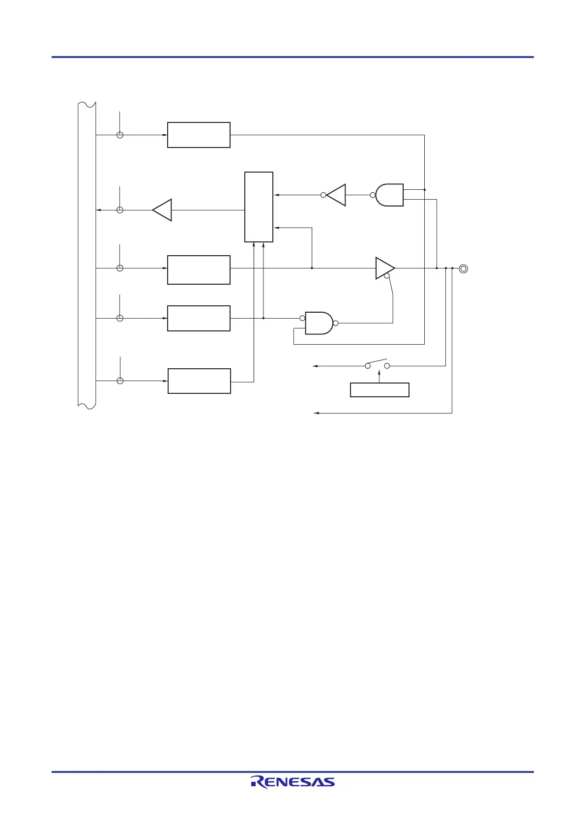
Figure 4-50. Block Diagram of P81
P81/ANI3
/
IVCMP00
WR
ADPC
RD
WR
PORT
WR
PM
ADPC
PM8
P8
PM81
P81
ADPC4 to ADPC0
WR
PMS
PMS
PMS0
Analog voltage
input for comparator
0: Analog input
1: Digital I/O
Internal bus
Output latch
Selector
A/D converter
ADS
ADS4 to ADS0
P8: Port register 8
PM8: Port mode register 8
PMS: Port mode select register
ADPC: A/D port configuration register
ADS: Analog input channel specification register
RD: Read signal
WRxx: Write signal

Table of Contents

Other manuals for Renesas RL78 Series

Questions and Answers:

Question and Answer IconNeed help?

Do you have a question about the Renesas RL78 Series and is the answer not in the manual?

Renesas RL78 Series Specifications

General IconGeneral
CoreRL78
CPU Clock SpeedUp to 32 MHz
Flash MemoryUp to 512 KB
RAMUp to 32 KB
Operating Voltage1.6 V to 5.5 V
Low Power ModesHALT, STOP, SNOOZE
CPU Architecture16-bit
Temperature Range-40°C to +85°C
PackageLQFP
Timers16-bit timers
Communication InterfacesUART, I2C, LIN
A/D Converter12-bit

Related product manuals