RL78/F13, F14 CHAPTER 6 TIMER ARRAY UNIT
R01UH0368EJ0210 Rev.2.10 472
Dec 10, 2015
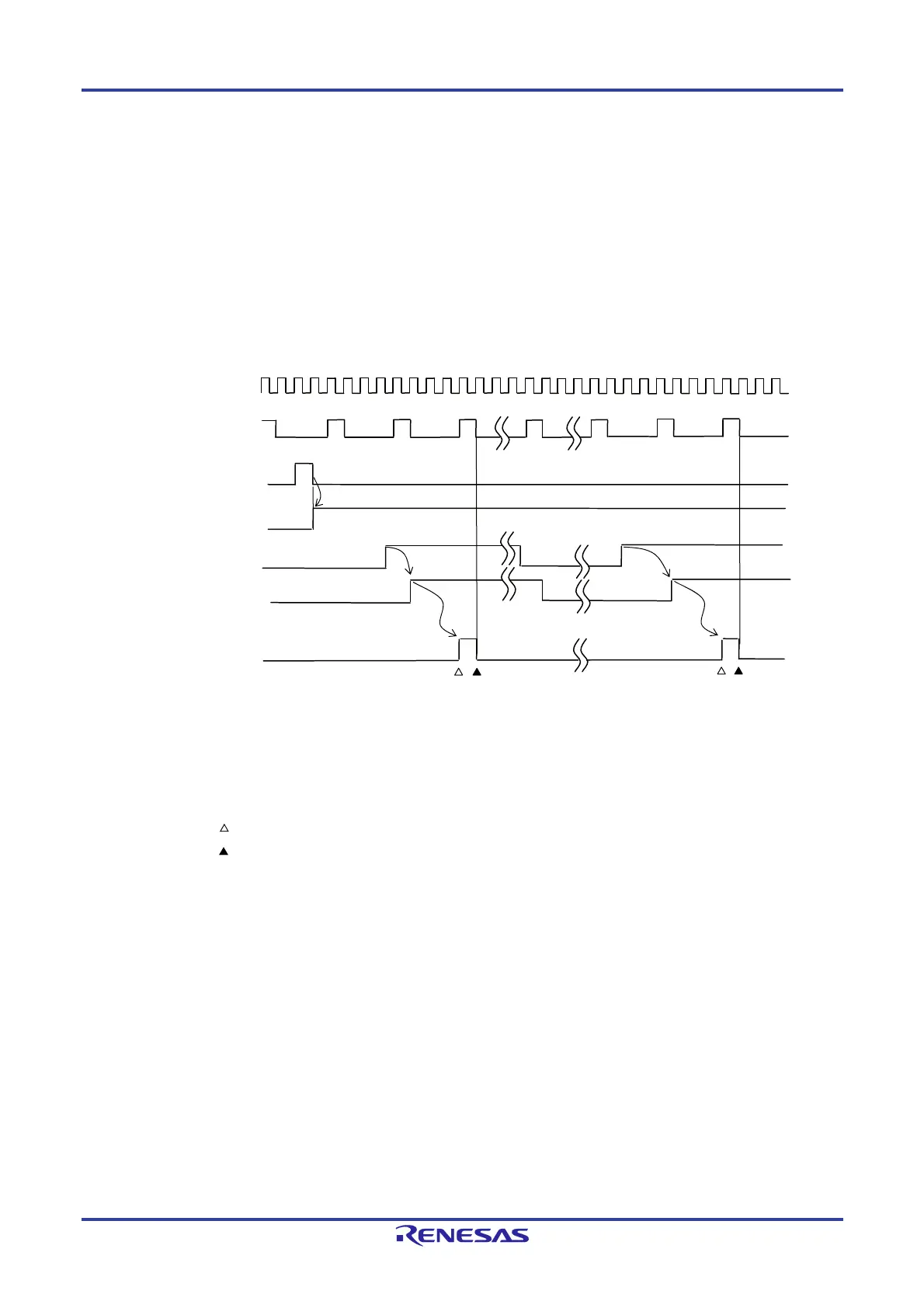
(2) When valid edge of input signal via the TImn pin is selected (CCSmn = 1)
The count clock (f
TCLK) becomes the signal that detects valid edge of input signal via the TImn pin and synchronizes
next rising f
MCK. The count clock (fTCLK) is delayed for 1 to 2 period of fMCK from the input signal via the TImn pin
(when a noise filter is used, the delay becomes 3 to 4 clock).
Counting of timer count register mn (TCRmn) delayed by one period of f
CLK from rising edge of the count clock,
because of synchronization with f
CLK. But, this is described as “counting at valid edge of input signal via the TImn
pin”, as a matter of convenience.
Figure 6-28. Timing of count clock (fTCLK) (When CCSmn = 1, noise filter unused)
<1> Setting TSmn bit to 1 enables the timer to be started and to become wait state for valid edge of input signal
via the TImn pin.
<2> The rise of input signal via the TImn pin is sampled by f
MCK.
<3> The edge is detected by the rising of the sampled signal and the detection signal (count clock) is output.
Remarks 1. : Rising edge of the count clock
: Synchronization, increment/decrement of counter
2. f
CLK: CPU/peripheral hardware clock
f
MCK: Operation clock of channel n
3. The waveform of the input signal via TImn pin of the input pulse interval measurement, the
measurement of high/low width of input signal, and the delay counter, and the one-shot pulse output
are the same as that shown in Figure 6-28.
f
MC
TSmn(Write)
TEmn
TImn input
<1>
<2>
Rising edge
detection signal (f
TCLK
)
Sampling wave
Edge detection
Edge detection
<3>
f
CL

 Loading...


