EasyManuals Logo

Renesas RL78 Series User Manual

Renesas RL78 Series
1879 pages
To Next Page IconTo Next Page
To Previous Page IconTo Previous Page
Page #532 background imageLoading...
Page #532 background image
RL78/F13, F14 CHAPTER 6 TIMER ARRAY UNIT
R01UH0368EJ0210 Rev.2.10 500
Dec 10, 2015
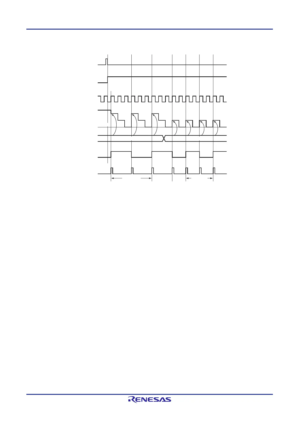
Figure 6-52. Example of Basic Timing of Operation as Frequency Divider (MDmn0 = 1)
Remark TS00: Bit n of timer channel start register m (TSm)
TE00: Bit n of timer channel enable status register m (TEm)
TI00: TI00 pin input signal
TCR00: Timer count register 00 (TCR00)
TDR00: Timer data register 00 (TDR00)
TO00: TO00 pin output signal
TS00
TE00
TI00
TDR00
TCR00
TO00
INTTM00
0002H
Divided
by 6
0001H
0
0000H
1
2
0
1
2
0
1
0
1
0
1
0
1
0
1
2
Divided
by 4

Table of Contents

Other manuals for Renesas RL78 Series

Questions and Answers:

Question and Answer IconNeed help?

Do you have a question about the Renesas RL78 Series and is the answer not in the manual?

Renesas RL78 Series Specifications

General IconGeneral
CoreRL78
CPU Clock SpeedUp to 32 MHz
Flash MemoryUp to 512 KB
RAMUp to 32 KB
Operating Voltage1.6 V to 5.5 V
Low Power ModesHALT, STOP, SNOOZE
CPU Architecture16-bit
Temperature Range-40°C to +85°C
PackageLQFP
Timers16-bit timers
Communication InterfacesUART, I2C, LIN
A/D Converter12-bit

Related product manuals