RL78/F13, F14 CHAPTER 8 TIMER RD
R01UH0368EJ0210 Rev.2.10 603
Dec 10, 2015
[PWM3 Mode]
Access registers TRDGRAi to TRDGRDi in 16-bit units. Do not access them in 8-bit units.
The following registers are disabled in PWM3 mode:
TRDPMR, TRDDF0, TRDDF1, TRDIORA0, TRDIORC0, TRDPOCR0, TRDIORA1, TRDIORC1, and TRDPOCR1
Registers TRDGRC0, TRDGRC1, TRDGRD0, and TRDGRD1 are not used in PWM3 mode. To use them as buffer
registers, set bits TRDBFC0, TRDBFC1, TRDBFD0, and TRDBFD1 to 0 (general register) and write a value to the TRDGRC0,
TRDGRC1, TRDGRD0, or TRDGRD1 register. After this, bits TRDBFC0, TRDBFC1, TRDBFD0, and TRDBFD1 may be set
to 1 (buffer register).
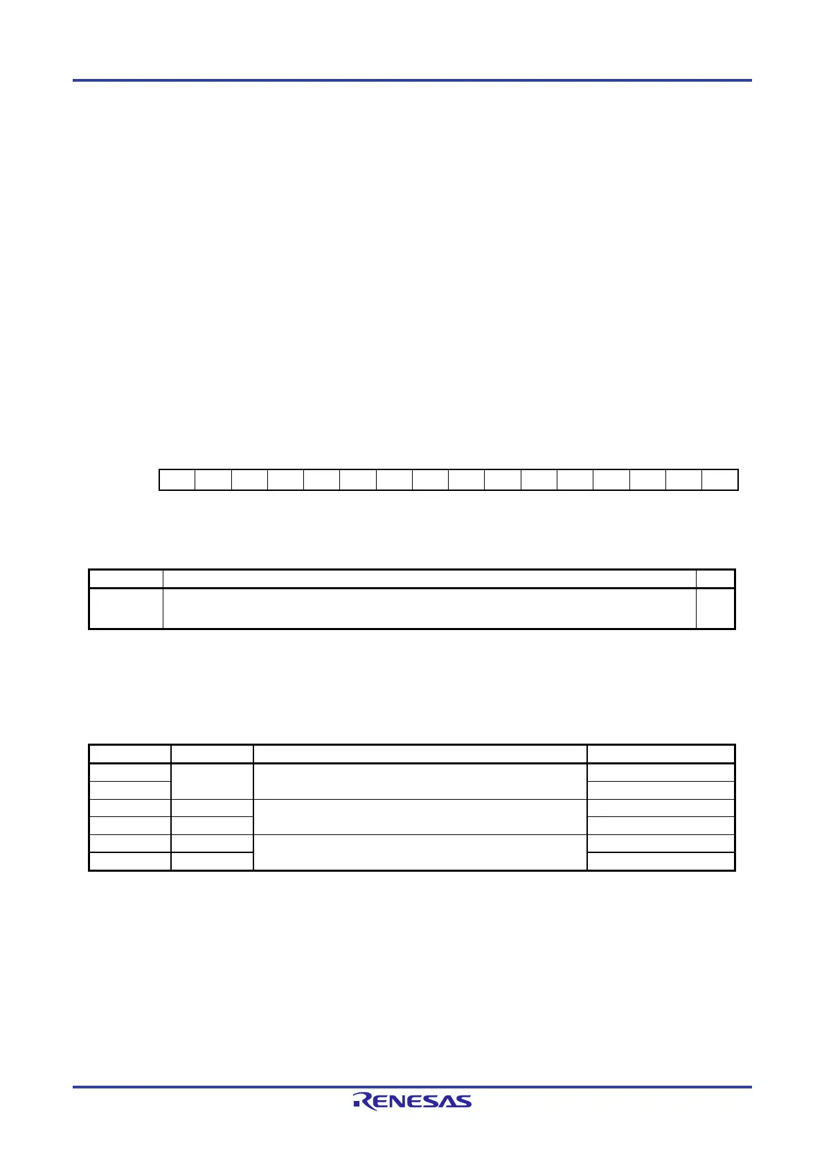
Figure 8-33. Format of Timer RD General Registers Ai, Bi, Ci, and Di (TRDGRAi, TRDGRBi,TRDGRCi, TRDGRDi)
(i = 0 or 1) [Input Capture Function]
Address: F0278H (TRDGRA0), F027AH (TRDGRB0), After Reset: FFFFH
Note
FFF58H (TRDGRC0), FFF5AH (TRDGRD0),
F0288H (TRDGRA1), F028AH (TRDGRB1),
FFF5CH (TRDGRC1), FFF5EH (TRDGRD1)
Symbol 15 14 13 12 11 10 9 8 7 6 5 4 3 2 1 0
TRDGRAi — — — — — — — — — — — — — — — —
TRDGRBi
TRDGRCi
TRDGRDi
— Function R/W
Bits 15 to 0 See Table 8-3 TRDGRji Register Functions in Input Capture Function. R/W
Note The value after reset is undefined when FRQSEL4 = 1 in the user option byte (000C2H/020C2H) and TRD0EN =
0 in the PER1 register. If it is necessary to read the initial value, set f
CLK to fIH and TRD0EN = 1 before reading.
Table 8-3. TRDGRji Register Functions in Input Capture Function
Register Setting Register Function Input-Capture Input Pin
TRDGRAi — General register. The value of the TRDi register can be read at
input capture.
TRDIOAi
TRDGRBi TRDIOBi
TRDGRCi TRDBFCi = 0 General register. The value of the TRDi register can be read at
input capture.
TRDIOCi
TRDGRDi TRDBFDi = 0 TRDIODi
TRDGRCi TRDBFCi = 1 Buffer register. The value of the TRDi register can be read at
input capture (see 8. 3. 1 (2) Buffer Operation).
TRDIOAi
TRDGRDi TRDBFDi = 1 TRDIOBi
Remark i = 0 or 1, j = A, B, C, or D
TRDBFCi, TRDBFDi: Bits in TRDMR register

 Loading...


