RL78/F13, F14 CHAPTER 8 TIMER RD
R01UH0368EJ0210 Rev.2.10 605
Dec 10, 2015
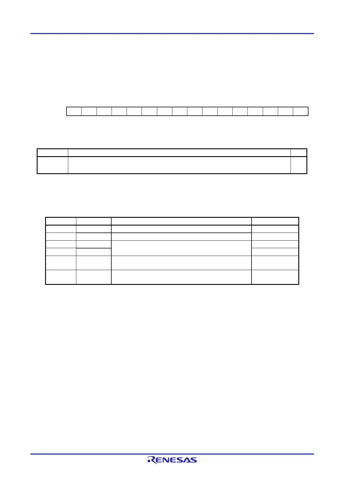
Figure 8-35. Format of Timer RD General Registers Ai, Bi, Ci, and Di (TRDGRAi, TRDGRBi,TRDGRCi, TRDGRDi)
(i = 0 or 1) [PWM Mode]
Address: F0278H (TRDGRA0), F027AH (TRDGRB0), After Reset: FFFFH
Note
FFF58H (TRDGRC0), FFF5AH (TRDGRD0),
F0288H (TRDGRA1), F028AH (TRDGRB1),
FFF5CH (TRDGRC1), FFF5EH (TRDGRD1)
Symbol 15 14 13 12 11 10 9 8 7 6 5 4 3 2 1 0
TRDGRAi — — — — — — — — — — — — — — — —
TRDGRBi
TRDGRCi
TRDGRDi
— Function R/W
Bits 15 to 0 See Table 8-5 TRDGRji Register Functions in PWM Function. R/W
Note The value after reset is undefined when FRQSEL4 = 1 in the user option byte (000C2H/020C2H) and TRD0EN =
0 in the PER1 register. If it is necessary to read the initial value, set f
CLK to fIH and TRD0EN = 1 before reading.
Table 8-5. TRDGRji Register Functions in PWM Function
Register Setting Register Function PWM Output Pin
TRDGRAi — General register. Set the PWM period. —
TRDGRBi — General register. Set the changing point of PWM output. TRDIOBi
TRDGRCi TRDBFCi = 0 General register. Set the changing point of PWM output. TRDIOCi
TRDGRDi TRDBFDi = 0 TRDIODi
TRDGRCi TRDBFCi = 1 Buffer register. Set the next PWM period
(see 8. 3. 1 (2) Buffer Operation).
—
TRDGRDi TRDBFDi = 1 Buffer register. Set the changing point of the next PWM output
(see 8. 3. 1 (2) Buffer Operation).
TRDIOBi
Caution When the setting of bits TCK2 to TCK0 in the TRDCRi register is 000B (f
CLK, fIH, fPLL, fSUB, and fIL) and
the compare value is set to 0000H, a request signal to the data transfer controller (DTC) and the event
link controller (ELC) is generated only once immediately after the count starts. When the compare
value is 0001H or higher, a request signal is generated each time a compare match occurs.
Remark i = 0 or 1, j = A, B, C, or D
TRDBFCi, TRDBFDi: Bits in TRDMR register

 Loading...


