RL78/F13, F14 CHAPTER 8 TIMER RD
R01UH0368EJ0210 Rev.2.10 631
Dec 10, 2015
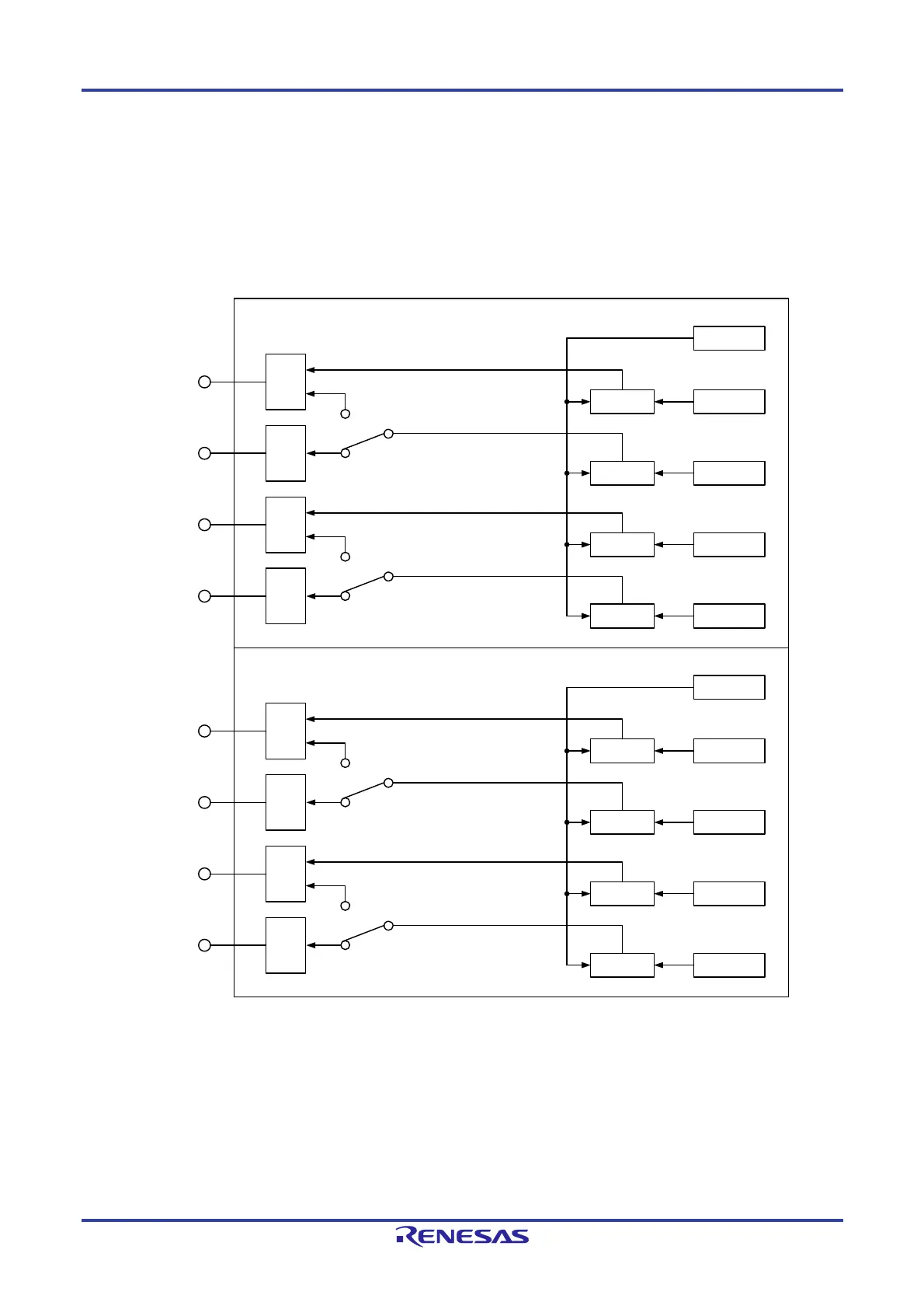
(2) Changing Output Pins in Registers TRDGRCi (i = 0 or 1) and TRDGRDi
The TRDGRCi register can be used for output control of the TRDIOAi pin, and the TRDGRDi register can be used
for output control of the TRDIOBi pin. Therefore, each pin output can be controlled as follows:
TRDIOAi output is controlled by the values in registers TRDGRAi and TRDGRCi.
TRDIOBi output is controlled by the values in registers TRDGRBi and TRDGRDi.
Figure 8-50. Changing Output Pins in Registers TRDGRCi and TRDGRDi
Change output pins in registers TRDGRCi and TRDGRDi as follows:
• Select 0 (TRDGRji register output pin is changed) using the IOj3 (j = C or D) bit in the TRDIORCi register.
• Set the TRDBFji bit in the TRDMR register to 0 (general register).
• Set different values in registers TRDGRCi and TRDGRAi. Also, set different values in registers TRDGRDi and
TRDGRBi.
TRDIOA0
Comparator
TRDGRA0
TRD0
TRDIOC0
TRDGRC0
Compare match signal
Compare match signal
Compare match signal
Compare match signal
Compare match signal
Compare match signal
Compare match signal
Compare match signal
TRDIOB0
TRDGRB0
TRDIOD0
TRDGRD0
TRDIOA1
TRDGRA1
TRD1
TRDIOC1
TRDGRC1
TRDIOB1
TRDGRB1
TRDIOD1
TRDGRD1
IOC3 = 1
IOD3 = 1
IOC3 = 1
IOD3 = 1
Timer RD0
Output
control
Output
control
Output
control
Output
control
Output
control
Output
control
Output
control
Output
control
IOC3 = 0 in
TRDIORC0 register
IOD3 = 0 in
TRDIORC0 register
IOC3 = 0 in
TRDIORC1 register
IOD3 = 0 in
TRDIORC1 register
Timer RD1
Comparator
Comparator
Comparator
Comparator
Comparator
Comparator
Comparator

 Loading...


