2.6.1.4. Rate Match FIFO for GbE
The rate match FIFO compensates frequency Part-Per-Million (ppm) differences
between the upstream transmitter and the local receiver reference clock up to 125
MHz ± 100 ppm difference.
Note: 200 ppm total is only true if calculated as (125 MHz + 100 ppm) - (125 MHz - 100
ppm) = 200 ppm. By contrast, (125 MHz + 0 ppm) - (125 MHz - 200 ppm) is out of
specification.
The GbE protocol requires the transmitter to send idle ordered sets /I1/ (/K28.5/
D5.6/) and /I2/ (/K28.5/D16.2/) during inter-packet gaps (IPG) adhering to the rules
listed in the IEEE 802.3-2008 specification.
The rate match operation begins after the synchronization state machine in the word
aligner indicates synchronization is acquired by driving the rx_syncstatus signal
high. The rate matcher deletes or inserts both symbols /K28.5/ and /D16.2/ of
the /I2/ ordered sets as a pair in the operation to prevent the rate match FIFO from
overflowing or underflowing. The rate match operation can insert or delete as
many /I2/ ordered sets as necessary.
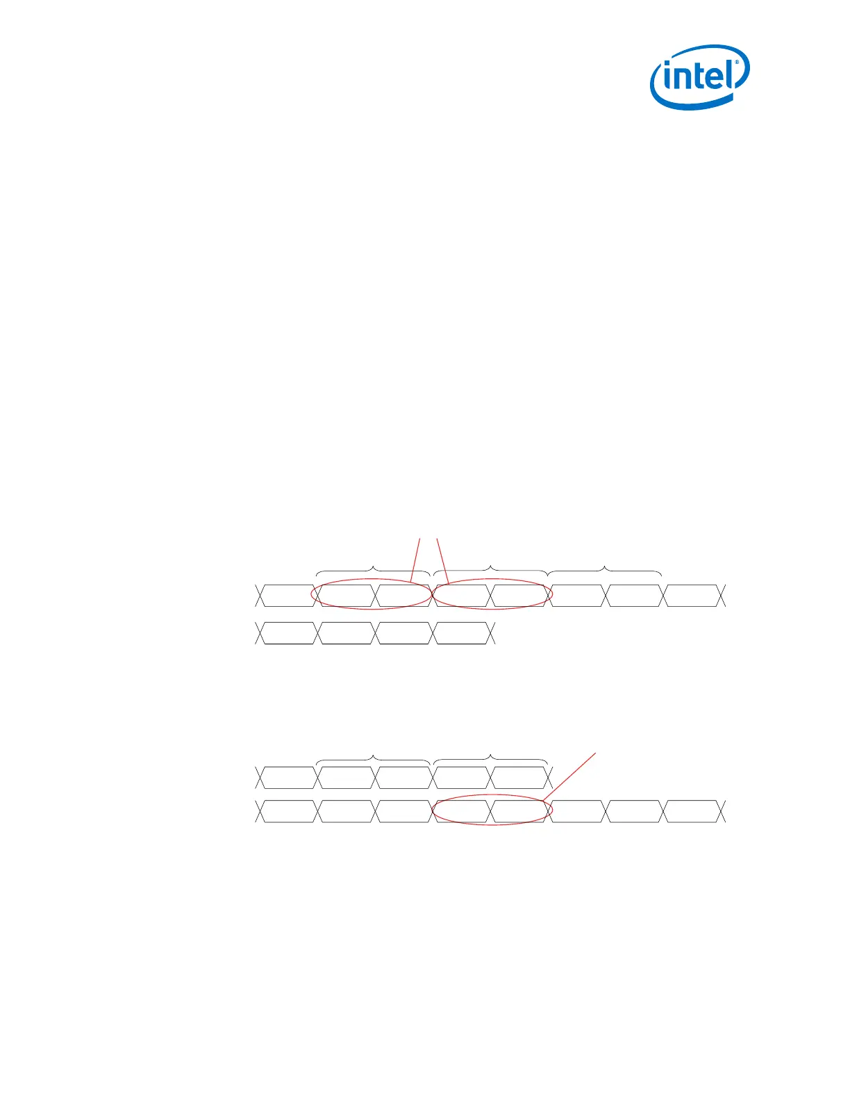
The following figure shows a rate match deletion operation example where three
symbols must be deleted. Because the rate match FIFO can only delete /I2/ ordered
sets, it deletes two /I2/ ordered sets (four symbols deleted).
Figure 48. Rate Match FIFO Deletion
Dx .y K 28 .5
datain
K 28 .5 D 16 .2
K 28 .5 D 16 .2 Dx .y
D 16 .2
First /I2/ Ordered S et /I2/ Ordered S etS econd Third /I2/ Ordered S et
Dx .y Dx .yK 28 .5dataout D 16 .2
/I2/ SKP Symbol Deleted
The following figure shows an example of rate match FIFO insertion in the case where
one symbol must be inserted. Because the rate match FIFO can only insert /I2/
ordered sets, it inserts one /I2/ ordered set (two symbols inserted).
Figure 49. Rate Match FIFO Insertion
Dx .y K 28 .5
datain
K 28 .5
K 28 .5
D 16 .2
K 28 .5 D 16 .2 Dx .y
D 16 .2
Dx .y K 28 .5dataout D 16 .2 D 16 .2
/I2/ SKP Symbol Inserted
First /I2/ Ordered Set Second /I2/ Ordered Set
rx_std_rmfifo_full and rx_std_rmfifo_empty are forwarded to the FPGA
fabric to indicate rate match FIFO full and empty conditions.
The rate match FIFO does not delete code groups to overcome a FIFO full condition. It
asserts the rx_std_rmfifo_full flag for at least two recovered clock cycles to
indicate rate match FIFO full. The following figure shows the rate match FIFO full
condition when the write pointer is faster than the read pointer.
2. Implementing Protocols in Arria 10 Transceivers
UG-01143 | 2018.06.15
Intel
®
Arria
®
10 Transceiver PHY User Guide
117