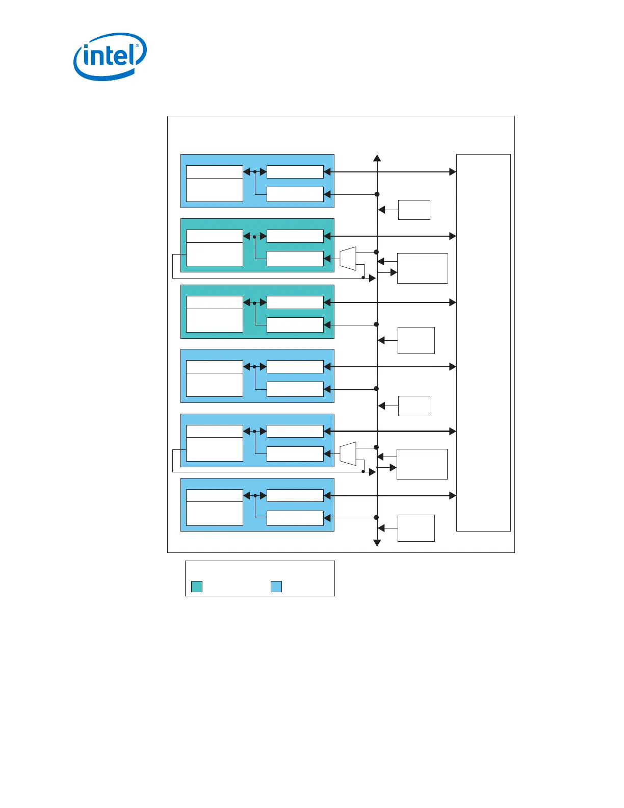
Figure 15. GT Transceiver Bank Architecture for Banks GXBL1E and GXBL1H
CH1
PMA
Channel PLL
(CDR Only)
PCS
Local CGB5
CH5
PMA
Channel PLL
(CMU/CDR)
PCS
Local CGB4
CH4
PMA
Channel PLL
(CDR Only)
PCS
Local CGB3
CH3
PMA
Channel PLL
(CDR Only)
PCS
Local CGB2
CH2
PMA
Channel PLL
(CMU/CDR)
PCS
Local CGB1
PMA
Channel PLL
(CDR Only)
PCS
Local CGB0
CH0
FPGA Core
Fabric
Clock
Distribution
Network
Six-Channel GT
Transceiver Banks GXBL1E and GXBL1H
fPLL1
Master
CGB1
Master
CGB0
ATX
PLL1
ATX
PLL0
fPLL0
GX Channel
GT/GX Channel
Legend
Note: This figure is a high level overview of the transceiver bank architecture. For details
about the available clock networks refer to the PLLs and Clock Networks chapter.
The transceiver channels perform all the required PHY layer functions between the
FPGA fabric and the physical medium. The high speed clock required by the
transceiver channels is generated by the transceiver PLLs. The master and local clock
generation blocks (CGBs) provide the necessary high speed serial and low speed
parallel clocks to drive the non-bonded and bonded channels in the transceiver bank.
1. Arria
®
10 Transceiver PHY Overview
UG-01143 | 2018.06.15
Intel
®
Arria
®
10 Transceiver PHY User Guide
24