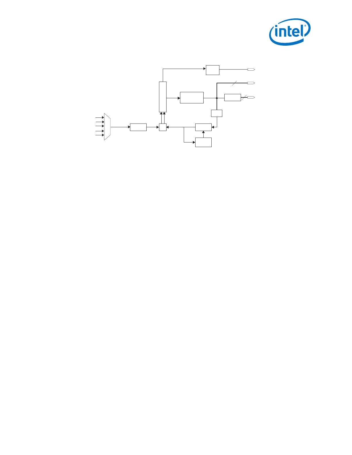
Figure 170. ATX PLL Block Diagram
VCO
Lock
Detector
PFD
CP &
LF
Refclk
Multiplexer
2
2
/2
M Counter
Delta Sigma
Modulator (1)
N Counter
L Counter
Reference clock network
M Counter
Note: (1) The Delta Sigma Modulator is enaged only when the ATX PLL is used in fractional mode.
Receiver input pin
Output of another PLL
with PLL cascading
Dedicated reference clock pin
DownUp
Global clock or core clock
pll_locked
refclk
fbclk
Input reference
clock
Input Reference Clock
This is the dedicated input reference clock source for the PLL.
The input reference clock can be sourced from one of the following:
• Dedicated reference clock pin
• Reference clock network
• Receiver input pin
• Output of another PLL with PLL cascading
• Global clock or the core clock network
The input reference clock to the dedicated reference clock pin is a differential signal.
Intel recommends using the dedicated reference clock pin as the input reference clock
source for the best jitter performance. The input reference clock must be stable and
free-running at device power-up for proper PLL operation and PLL calibration. If the
reference clock is not available at device power-up, then you must recalibrate the PLL
when the reference clock is available.
Note: Sourcing reference clock from a cascaded PLL output, global clock or core clock
network introduces additional jitter to the ATX PLL output. Refer to KDB "How do I
compensate for the jitter of PLL cascading or non-dedicated clock path for Arria 10 PLL
reference clock?" for more details.
The ATX PLL calibration is clocked by the CLKUSR clock which must be stable and
available for calibration to proceed. Refer to the Calibration section for more details
about the CLKUSR clock.
Reference Clock Multiplexer
The reference clock (refclk) multiplexer selects the reference clock to the PLL from
the various reference clock sources available.
N Counter
The N counter divides the refclk mux's output. The division factors supported are 1,
2, 4, and 8.
3. PLLs and Clock Networks
UG-01143 | 2018.06.15
Intel
®
Arria
®
10 Transceiver PHY User Guide
351