The following table shows the addresses and bits for transmitter PLL switching. The
number of exposed tx_serial_clk bits varies according to the number of
transmitter PLLs you specify. Use the Native PHY reconfiguration interface for this
operation.
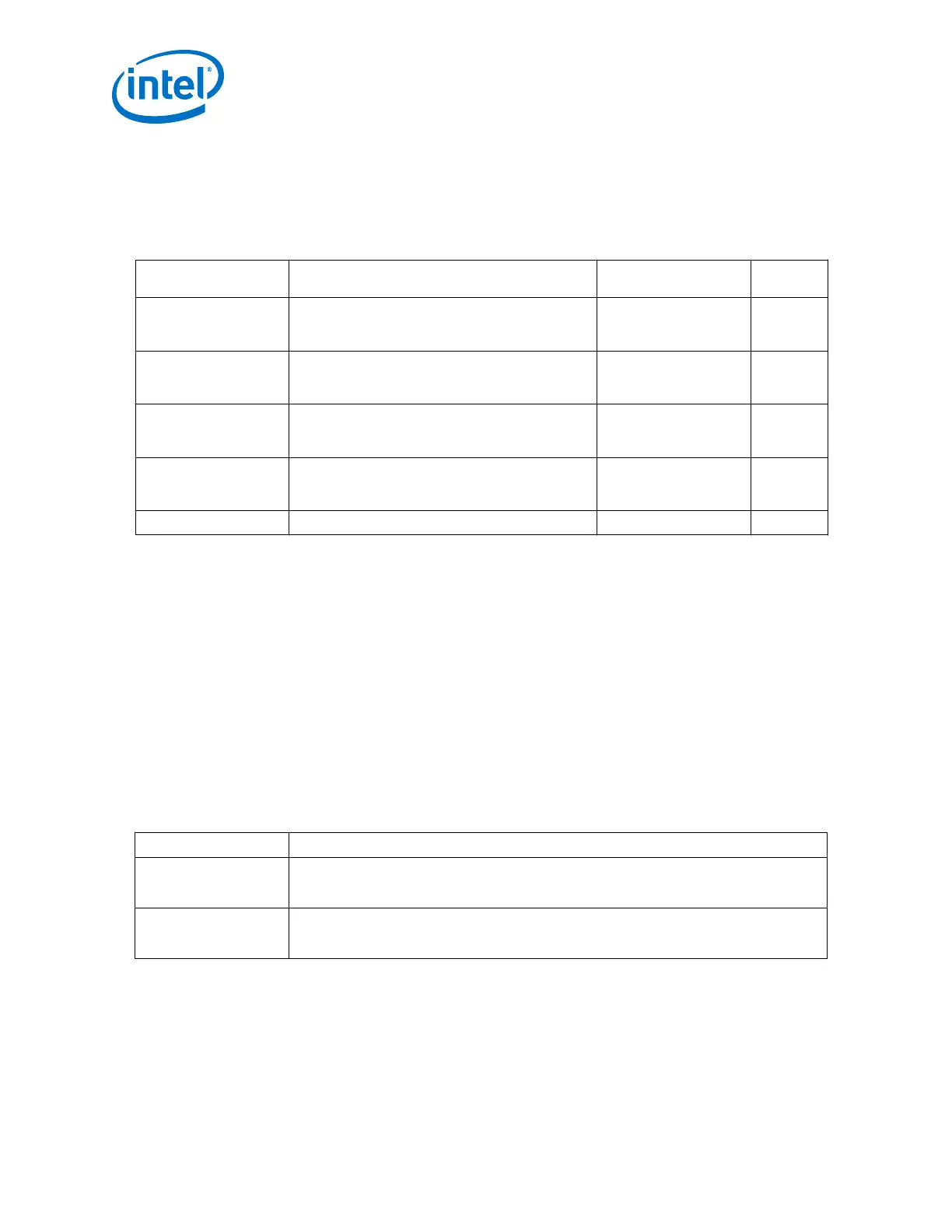
Table 267. Register Map for Switching Transmitter PLLs
Transceiver Native PHY
Port
Description Address Bits
tx_serial_clk0 Represents logical PLL0. Lookup register x117[3:0]
stores the mapping from logical PLL0 to the physical
PLL.
0x117 (Lookup Register) [3:0]
tx_serial_clk1 Represents logical PLL1. Lookup register x117[7:4]
stores the mapping from logical PLL1 to the physical
PLL.
0x117 (Lookup Register) [7:4]
tx_serial_clk2 Represents logical PLL2. Lookup register x118[3:0]
stores the mapping from logical PLL2 to the physical
PLL.
0x118 (Lookup Register) [3:0]
tx_serial_clk3 Represents logical PLL3. Lookup register x118[7:4]
stores the mapping from logical PLL3 to the physical
PLL.
0x118 (Lookup Register) [7:4]
N/A PLL selection MUX 0x111 [7:0]
When performing a PLL switch, you must specify the lookup register address and bit
values you want to switch to. The following procedure describes selection of a specific
transmitter PLL when more than one PLL is connected to a channel. To change the
data rate of the CDR, follow the detailed steps for reconfiguring channel and PLL
blocks. After determining the logical PLL to switch to, follow this procedure to switch
to the desired transmitter PLL:
1. Perform the necessary steps from steps 1 to 7 in Steps to Perform Dynamic
Reconfiguration.
2. Read from the appropriate lookup register address (refer to Table 267 on page
522) and save the required 4-bit pattern. For example, switching to logical PLL1
requires saving bits [7:4] of address 0x117.
3. Encode the 4-bit value read in the previous step into an 8-bit value according to
the following table:
Table 268. Logical PLL Encoding
4-bit Logical PLL Bits 8-bit Mapping to Address 0x111
[3..0] {~logical_PLL_offset_readdata[3],
logical_PLL_offset_readdata[1:0],logical_PLL_offset_readdata[3],
logical_PLL_offset_readdata[3:0] }
[7..4] {~logical_PLL_offset_readdata[7],
logical_PLL_offset_readdata[5:4],logical_PLL_offset_readdata[7],
logical_PLL_offset_readdata[7:4] }
6. Reconfiguration Interface and Dynamic Reconfiguration
UG-01143 | 2018.06.15
Intel
®
Arria
®
10 Transceiver PHY User Guide
522