In the following tables, the variables represent these parameters:
• <n>—The number of lanes
• <w>—The width of the interface
• <d>—The serialization factor
• <s>— The symbol size
• <p>—The number of PLLs
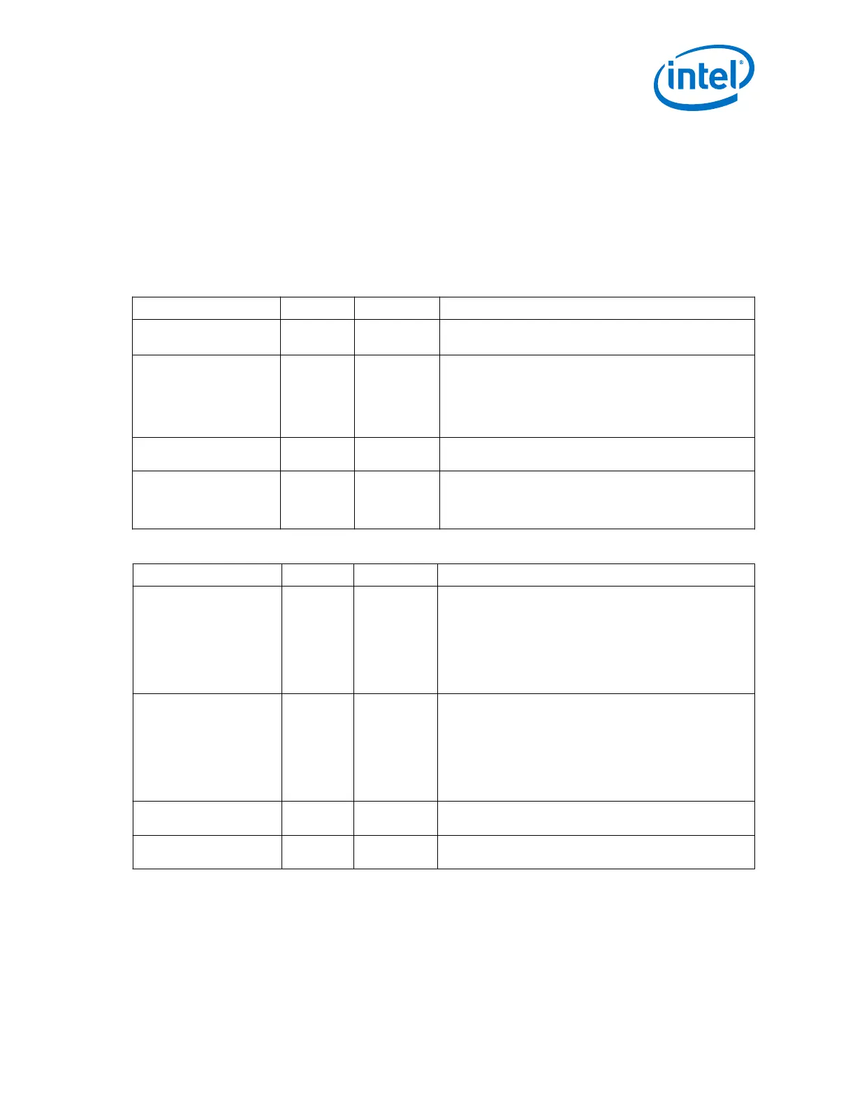
Table 68. TX Standard PCS: Data, Control, and Clocks
Name Direction Clock Domain Description
tx_parallel_data[<n>
128-1:0]
Input
tx_clkout
TX parallel data input from the FPGA fabric to the TX PCS.
unused_tx_parallel_d
ata
Input
tx_clkout
This signal specifies the unused data when you turn on
Enable simplified data interface. When simplified data
interface is not set, the unused bits are a part of
tx_parallel_data. Connect all these bits to 0. If you do
not connect the unused data bits to 0, then TX parallel data
may not be serialized correctly by the Native PHY IP core.
tx_coreclkin
Input Clock The FPGA fabric clock. This clock drives the write port of the
TX FIFO.
tx_clkout
Output Clock This is the parallel clock generated by the local CGB for non
bonded configurations, and master CGB for bonded
configuration. This clocks the tx_parallel_data from the
FPGA fabric to the TX PCS.
Table 69. RX Standard PCS: Data, Control, Status, and Clocks
Name Direction Clock Domain Description
rx_parallel_data[<n>
128-1:0]
Output Synchronous
to the clock
driving the
read side of
the FIFO
(rx_coreclk
in or
rx_clkout)
RX parallel data from the RX PCS to the FPGA fabric. For
each 128-bit word of rx_parallel_data, the data bits
correspond to rx_parallel_data[7:0] when 8B/10B
decoder is enabled and rx_parallel_data[9:0] when
8B/10B decoder is disabled.
unused_rx_parallel_da
ta
Output Synchronous
to the clock
driving the
read side of
the FIFO
(rx_coreclk
in or
rx_clkout)
This signal specifies the unused data when you turn on
Enable simplified data interface. When simplified data
interface is not set, the unused bits are a part of
rx_parallel_data. These outputs can be left floating.
rx_clkout
Output Clock The low speed parallel clock recovered by the transceiver RX
PMA, that clocks the blocks in the RX Standard PCS.
rx_coreclkin
Input Clock RX parallel clock that drives the read side clock of the RX
FIFO.
2. Implementing Protocols in Arria 10 Transceivers
UG-01143 | 2018.06.15
Intel
®
Arria
®
10 Transceiver PHY User Guide
87