EasyManuals Logo

Renesas RL78 Series User Manual

Renesas RL78 Series
1879 pages
To Next Page IconTo Next Page
To Previous Page IconTo Previous Page
Page #296 background imageLoading...
Page #296 background image
RL78/F13, F14 CHAPTER 4 PORT FUNCTIONS
R01UH0368EJ0210 Rev.2.10 264
Dec 10, 2015
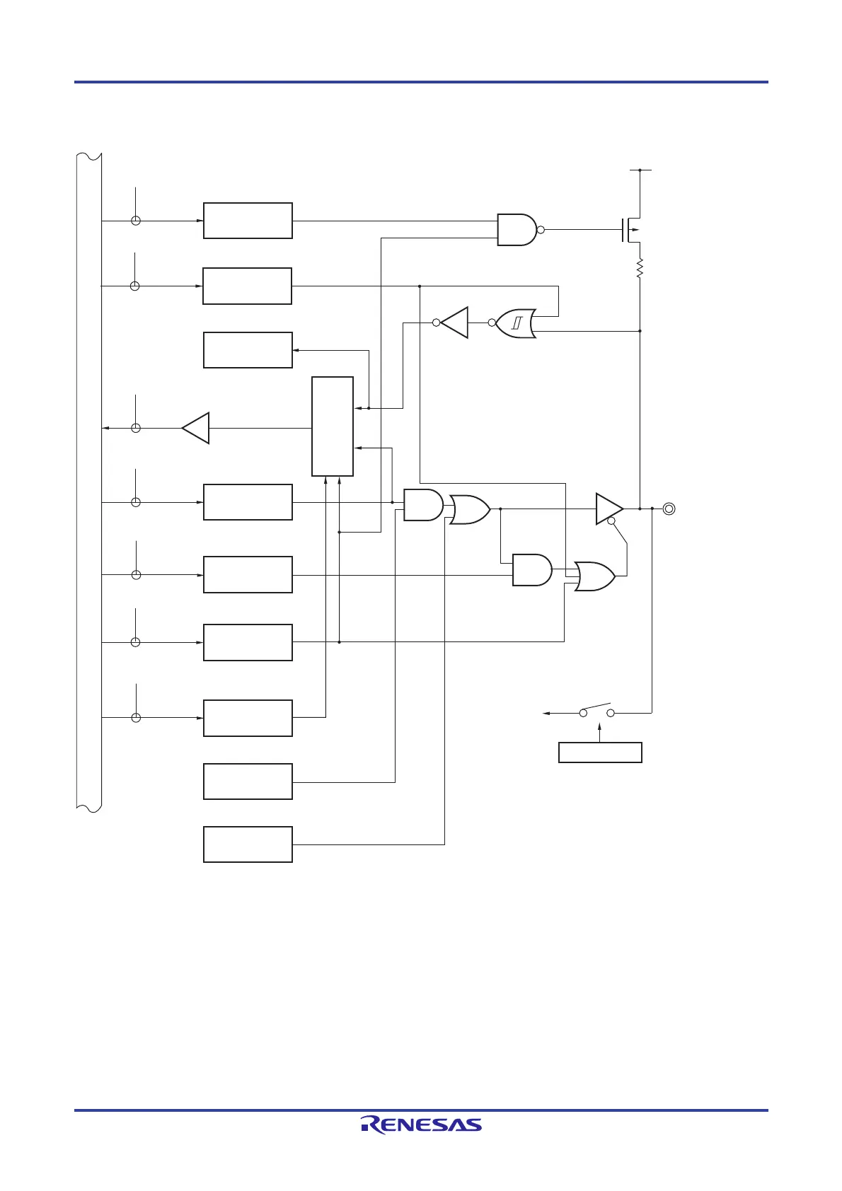
Figure 4-43. Block Diagram of P72
P72/ANI28/KR2
/
(CTXD0)/SO11/
SNZOUT6
WR
PU
RD
WR
PORT
PU72
(KR2)
P72
EV
DD
P-ch
PU7
P7
WR
PM
PM7
POM72
POM7
WR
POM
PM72
WR
PMC
PMC7
PMC72
WR
PMS
PMS
PMS0
SNZOUT6
SO11/(CTXD0)
Internal bus
Output latch
Alternate function
Alternate function
Alternate function
Selector
A/D converter
ADS
ADS4 to ADS0
P7: Port register 7
PU7: Pull-up resistor option register 7
PM7: Port mode register 7
POM7: Port output mode register 7
PMC7: Port mode control register 7
PMS: Port mode select register
ADS: Analog input channel specification register
RD: Read signal
WRxx: Write signal

Table of Contents

Other manuals for Renesas RL78 Series

Questions and Answers:

Question and Answer IconNeed help?

Do you have a question about the Renesas RL78 Series and is the answer not in the manual?

Renesas RL78 Series Specifications

General IconGeneral
CoreRL78
CPU Clock SpeedUp to 32 MHz
Flash MemoryUp to 512 KB
RAMUp to 32 KB
Operating Voltage1.6 V to 5.5 V
Low Power ModesHALT, STOP, SNOOZE
CPU Architecture16-bit
Temperature Range-40°C to +85°C
PackageLQFP
Timers16-bit timers
Communication InterfacesUART, I2C, LIN
A/D Converter12-bit

Related product manuals