Serial peripheral interface (SPI) RM0351
1444/1830 DocID024597 Rev 5
42.6.4 SPI data register (SPIx_DR)
Address offset: 0x0C
Reset value: 0x0000
42.6.5 SPI CRC polynomial register (SPIx_CRCPR)
Address offset: 0x10
Reset value: 0x0007
Note: The polynomial value should be odd only. No even value is supported.
Bits 3:2 Reserved, must be kept at reset value.
Bit 1 TXE: Transmit buffer empty
0: Tx buffer not empty
1: Tx buffer empty
Bit 0 RXNE: Receive buffer not empty
0: Rx buffer empty
1: Rx buffer not empty
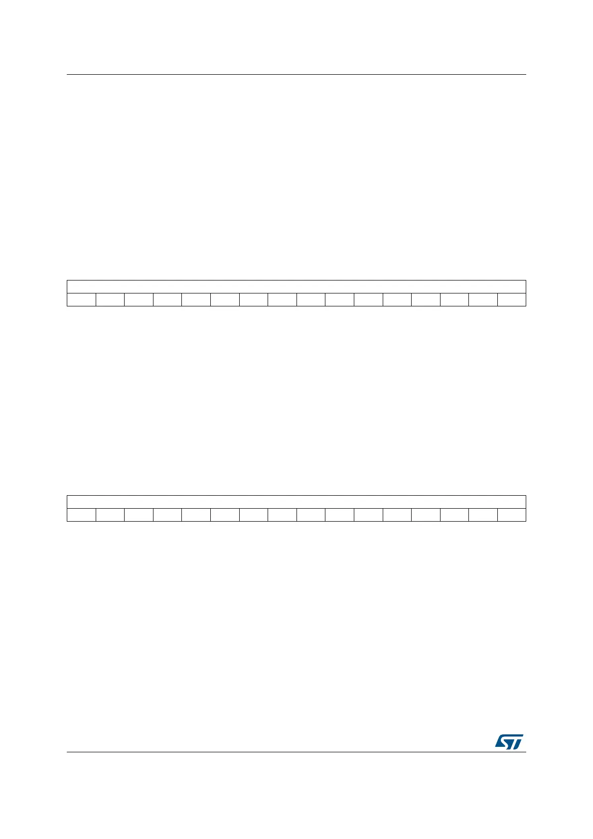
1514131211109876543210
DR[15:0]
rw rw rw rw rw rw rw rw rw rw rw rw rw rw rw rw
Bits 15:0 DR[15:0]: Data register
Data received or to be transmitted
The data register serves as an interface between the Rx and Tx FIFOs. When the data
register is read, RxFIFO is accessed while the write to data register accesses TxFIFO (See
Section 42.4.9: Data transmission and reception procedures).
Note: Data is always right-aligned. Unused bits are ignored when writing to the register, and
read as zero when the register is read. The Rx threshold setting must always
correspond with the read access currently used.
1514131211109876543210
CRCPOLY[15:0]
rw rw rw rw rw rw rw rw rw rw rw rw rw rw rw rw
Bits 15:0 CRCPOLY[15:0]: CRC polynomial register
This register contains the polynomial for the CRC calculation.
The CRC polynomial (0007h) is the reset value of this register. Another polynomial can be
configured as required.
 Loading...


