DocID024597 Rev 5 215/1830
RM0351 Reset and clock control (RCC)
278
configuration register (RCC_CFGR).
• LSCO
Another output (LSCO) allows a low speed clock to be output onto the external LSCO
pin:
–LSI
–LSE
This output remains available in Stop (Stop 0, Stop 1 and Stop 2) and Standby modes.
The selection is controlled by the LSCOSEL, and enabled with the LSCOEN in the
Backup domain control register (RCC_BDCR).
The configuration registers of the corresponding GPIO port must be programmed in
alternate function mode.
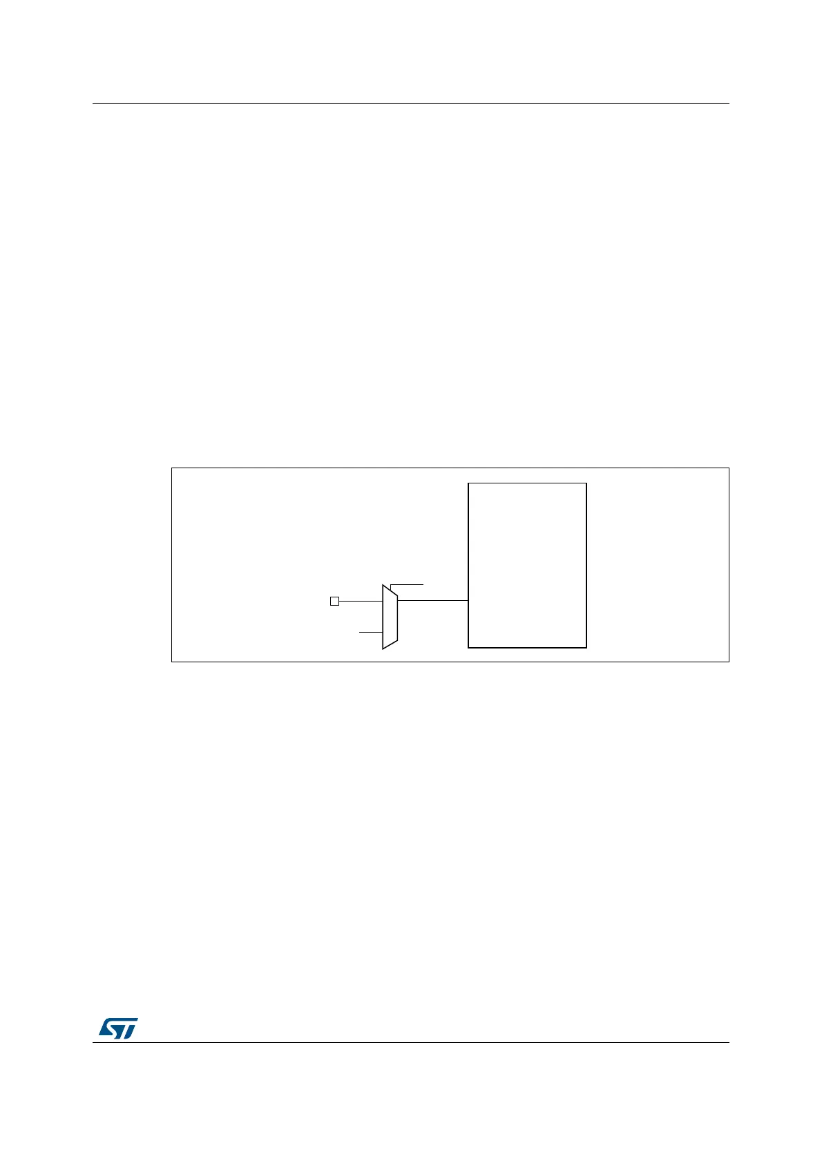
6.2.18 Internal/external clock measurement with TIM15/TIM16/TIM17
It is possible to indirectly measure the frequency of all on-board clock sources by mean of
the TIM15, TIM16 or TIM17 channel 1 input capture, as represented on Figure 18, Figure 19
and Figure 20.
Figure 18. Frequency measurement with TIM15 in capture mode
The input capture channel of the Timer 15 can be a GPIO line or an internal clock of the
MCU. This selection is performed through the TI1_RMP bit in the TIM15_OR register. The
possibilities are the following ones:
• TIM15 Channel1 is connected to the GPIO. Refer to the alternate function mapping in
the device datasheets.
• TIM15 Channel1 is connected to the LSE.
069
7,0
7,
7,B503
*3,2
/6(
 Loading...


