DocID024597 Rev 5 473/1830
RM0351 Quad-SPI interface (QUADSPI)
500
17.4 QUADSPI functional description
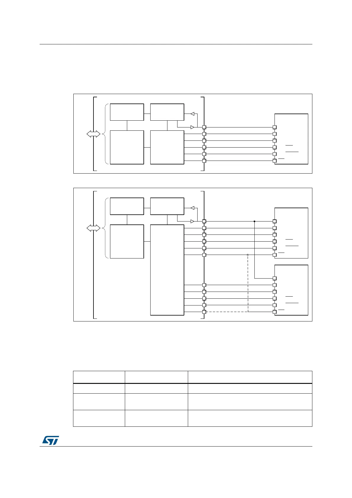
17.4.1 QUADSPI block diagram
Figure 58. QUADSPI block diagram when dual-flash mode is disabled
Figure 59. QUADSPI block diagram when dual-flash mode is enabled
17.4.2 QUADSPI pins
Table 99 lists the QUADSPI pins, six for interfacing with a single Flash memory, or 10 to 11
for interfacing with two Flash memories (FLASH 1 and FLASH 2) in dual-flash mode.
63,)/$6+
069
&/.
%.B,262
%.B,26,
%.B,2
%.B,2
&/.
46,
462
4:3
4+2/'
%.BQ&6
&6
$+%
5HJLVWHUV
FRQWURO
&ORFN
PDQDJHPHQW
),)2 6KLIWUHJLVWHU
48$'63,
069
63,)/$6+
&/.
%.B,262
%.B,26,
%.B,2
%.B,2
&/.
46,
462
4:3
4+2/'
%.BQ&6
&6
$+%
5HJLVWHUV
FRQWURO
&ORFN
PDQDJHPHQW
),)2
6KLIWUHJLVWHU
48$'63,
%.B,262
%.B,26,
%.B,2
%.B,2
%.BQ&6
63,)/$6+
&/.
46,
462
4:3
4+2/'
&6
Table 99. QUADSPI pins
Signal name Signal type Description
CLK Digital output Clock to FLASH 1 and FLASH 2
BK1_IO0/SO Digital input/output
Bidirectional IO in dual/quad modes or serial output
in single mode, for FLASH 1
BK1_IO1/SI Digital input/output
Bidirectional IO in dual/quad modes or serial input
in single mode, for FLASH 1
 Loading...


